Announcements
Imaging
NEW! GMOS-S detector array has been upgraded. CCD1 and CCD2 have been replaced by new Hamamatsu chips (of similar type to the original ones). The commissioning is ongoing, as it had to be interrupted due to the cybersecurity incident. It will be resumed once the telescope is back online.
GMOS can perform broad band imaging (using the SDSS filter system) or narrow-band imaging using selected filters. The field of view is 5.5 arcmin x 5.5 arcmin (and does not cover the entire CCD package).
The GMOS-S original EEV CCDs, GMOS-N original EEV CCDs, and upgraded GMOS-N e2v DD devices had two ~ 2.8 arcsec (39 pixel)-wide chip gaps, as shown in the image below. To cover the gaps it is recommended to use dither steps of at least 5 arcsec in the X-direction.
On the new Hamamatsu CCDs at GMOS-S the two gaps are 4.88 arcsec wide (61 pixels in unbinned mode). The inter-chip gaps for the GMOS-N Hamamatsu CCDs are 5.4 arcsec wide (67 pixels in unbinned mode). Due to bright edges at either side of the chip gaps, it is recommended to use dither steps of 10 arcsec in the X-direction to cover the gaps of the GMOS-S and GMOS-N Hamamatsu CCDs.
Camera Properties
-
Instrument Pixel Size
(arcsec)Imaging Field of View
(arcsec2)Throughput GMOS-N (original EEV and
upgraded e2v DD)0.0728 330 x 330 data / plot GMOS-N (Hamamatsu) 0.0807 330 x 330 data / plot GMOS-S (original EEV) 0.073 330 x 330 data / plot GMOS-S (Hamamatsu) 0.080 330 x 330 data / plot
Spectroscopy
Three types of spectroscopy are possible with each GMOS and its selection of gratings.
- Long-slit spectroscopy, which covers the full extent of the CCD package (3 x 2048 pixels) with two small gaps.
- Multi-object spectroscopy, which uses custom-designed, laser-milled masks.
- Integral field spectroscopy, which uses 0.2 arcsec fibers covering a 35 square arcsec field of view.
Each of these modes has a separate section in the GMOS pages. Only the gratings and filters used by all three modes and the detector properties are described in this section.
The spectral resolving powers available range from about 500 (for the widest slits used on extended objects) to 4400 with a slit width of 0.5 arcsec, and 8800 with the (narrowest) 0.25 arcsec slit. Note that in normal seeing conditions slit losses will be very large for the narrowest slits.
The GMOS gratings exhibit scattered light, the level of which varies with wavelength and grating. Some example spectral images and potential strategies to mitigate the effects of scattered light on science data are given here.
Long-slit spectroscopy
Long slit spectroscopy can be obtained in either normal or Nod-and-Shuffle modes using GMOS standard slits or custom slits.
The dispersion direction of GMOS is along the rows of the image. Thus, the gaps between the detectors cause small gaps in the wavelength interval covered by a single observation. The GMOS-S original EEV CCDs, GMOS-N original EEV CCDs, and upgraded GMOS-N e2v DD devices had two ~2.8 arcsec (39 pixel) gaps. The inter-chip gaps between the new Hamamatsu detectors are 4.88 arcsec wide (61 pixels in unbinned mode) for GMOS-S and 5.41 arcsec wide (67 pixels in unbinned mode) for GMOS-N. For both Hamamatsu detectors arrays, the effective chip gap width, not usable for science, is wider than the physical chip gap size due to bright edges at either side of the chip gaps. The equivalent gap in the wavelength coverage depends on the grating used for the observation. More information and recommended wavelength dither step sizes are provided in the Observing strategies section.
The longest wavelengths are at small X pixel coordinates in the first extension (extension [1]), the shortest wavelengths are at large X pixel coordinates in the last extension ([12] in the Hamamatsus, [6] in the e2vDD's, and [3] in the older E2V's). Thus, when the image has been displayed with gdisplay or mosaiced together with gmosaic the longest wavelengths are to the left and the shortest wavelengths to the right. The figures below show example longslit spectra with the wavelength direction and the gaps marked.
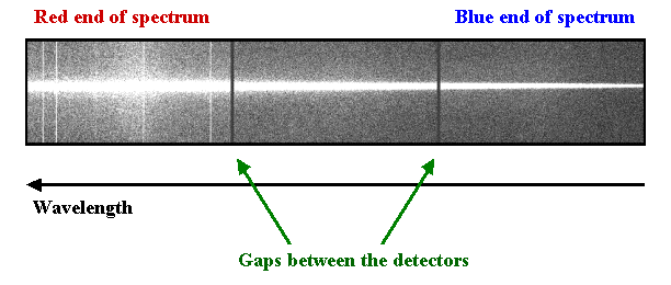
A typical GMOS observation of a spectrophotometric standard star. Only the central ~75 arcsec of the field of view are read out for this type of observation. The gaps between the detectors are shown.
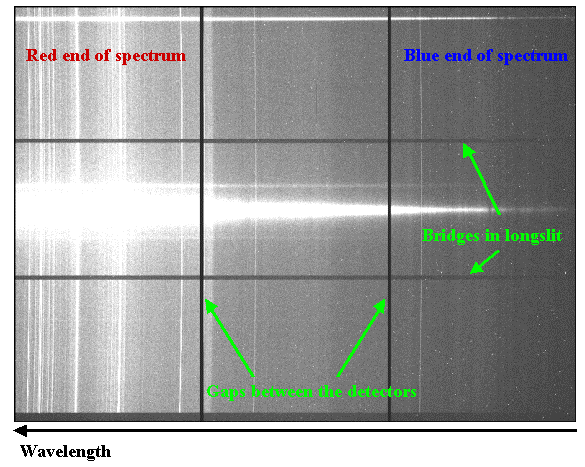
A GMOS longslit observation of a nearby galaxy. The full detector array is read out. The gaps between the detectors are shown. The longslits have bridges, causing small gaps in the spatial coverage. These bridges are necessary in order to keep the slit stable.
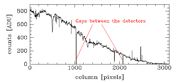
The average of the central 20 rows of the galaxy spectrum shown above. An approximate sky subtraction has been applied. No wavelength calibration or flux calibration have been applied. The gaps between the detectors are shown.
Multi-object spectroscopy
The multi-object mode of GMOS offers the possibility of obtaining spectra of several hundred objects simultaneously. The GMOS MOS design is based upon precisely fabricating and locating a plate containing many small slits within the spectrograph's entrance aperture. With a 5.5 square arcmin field of view, 30-60 slits can typically be located in a single mask, with a maximum of several hundred slits when narrow-band filters are used. A total of 9 MOS masks (plus the IFU) can be loaded into GMOS at any given time (maximum of 18 MOS masks in very exceptional cases, requiring to remove longlist masks). Actual mask production is done with laser cutting systems located in La Serena and Hilo. Currently masks are cut at both sites, Gemini North and Gemini South.
Currently offered capabilities:
- Slit widths 0.5 arcsec or larger
- Masks designed from GMOS direct imaging
- Masks designed from object catalogs
See information about:
- Mask preparation strategies
- Multi-Object spectroscopy resources
- Mask design
- Mask-making software
- Checking your mask design
- Mask deadlines (linked from the Phase II deadline for all instruments)
- Observing strategies
Integral Field Spectroscopy
The integral field mode of GMOS provides the ability to perform spatially resolved spectroscopy. This mode uses a lenslet array (containing 1500 elements) in the pre-slit environment to slice the focal plane into a multitude of small components. Each lenslet is coupled to a fiber. The fibers are organized into a linear array terminating at the nominal location of the slit of the spectrograph. It is possible to reconstruct an image at a particular wavelength, or extract a spectrum from any point in the field of view. The science field of view is 35 square arcsec (5"x7") and is sampled by 1000 elements. The sky is sampled by the remaining 500 elements which are located ~1 arcmin away from the science field of view. The GMOS-N IFU has been available since early 2002. The GMOS-S IFU has been available for science use since April 1, 2004.
In the future the IFU mode may be commissioned for use with Adaptive Optics. The mode is well suited for AO since it makes optimal use of the AO-corrected field, unlike a slit which blocks much of the corrected field. Currently, the Altair AO facility instrument on Gemini North only transmits light longward of 835 nm to the science instruments, so the GMOS-N would only have access to a limited wavelength range.
Because there is no Atmospheric Dispersion Corrector installed in either GMOS-N or GMOS-S, observers of extended sources should be aware that when observing in the blue or with the one-slit mode (to obtain wider wavelength coverage) different wavelengths may fall on different lenslets, especially at high airmass. It is possible to correct for this effect in data reduction using the GMOS IRAF package.
- Basic design
- Field-to-slit mapping
- Spectral Overlap in 2-slit mode
- R150 zero-order contamination in 2-Slit Mode
- Performance
- Observing strategies
IFU Basic Design
| Lenslet/fiber design | Hexagonal lenslets fully sample the FOV, fibers redirect the light to "slits" for effective detector use | |
| Easy deployment | Slides into the focal plane similar to a slit mask | |
| Wavelength range | 0.4-1.1 microns | |
| IFU format | Two fields separated by 1 arcminute | |
| Projected diameter of individual lenses | 0.2" | |
| Two-slit mode | all fibers used (half in each field) for maximum FOV, but with limited spectral coverage | |
| One-slit mode | half the number of fibers and FOV for extended wavelength coverage | |
| Fields of View (FOV): | two-slit mode: | one-slit mode: |
| "Object" FOV | 5" x 7" (1000 lenslets) | 5" x 3.5" (500 lenslets) |
| Nod & Shuffle FOV (GMOS-S only) | 5" x 5" (700 lenslets) | 5" x 2.5" (350 lenslets) |
| "Sky" FOV | 5" x 3.5" (500 lenslets) | 5" x 1.75" (250 lenslets) |
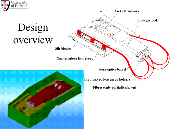
The overall design of the IFU is shown below. The IFU is stored in one of the three mask cassette slots and it is inserted into the beam as if it were a slit mask. Two pick-off mirrors direct light from the focal plane through fore-optics in the enlarger body and onto the lenslet arrays. Fibers then reformat the focal plane into two pseudo-slits that pass the light into the rest of the spectrograph. Either of these slits can be masked off in order to get more wavelength coverage but half the field-of-view ("one-slit" mode). The GMOS-S IFU also includes masks for allowing use of Nod & Shuffle.
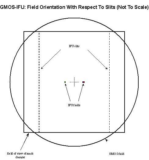
The figure below shows the relative positions of the IFU fields and the pseudo-slits in the focal plane. The slits are separated by 175mm. In two-slit mode the long axis of the 'Object' lenslet array is aligned with the dispersion axis of the spectrograph (along the x-axis of the CCDs).
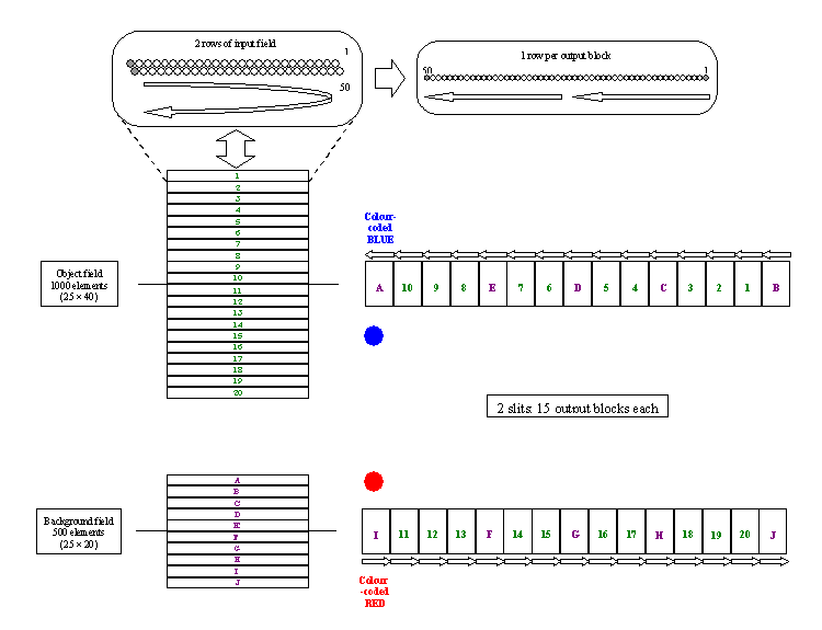
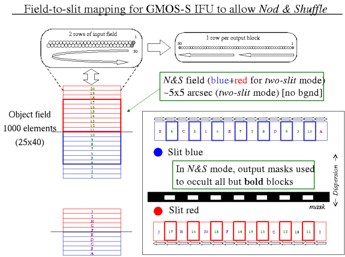
The lenslets are hexagonal in shape and are laid out in rows of 25 lenslets each. Pairs of rows are grouped into "slit blocks" of 50 fibers at the pseudo-slits. The nomenclature for the slit blocks, their locations in the IFU fields, and their mapping onto the detector are illustrated below. Note that the 'sky' lenslets (letters coded purple) are interleaved with the 'object' lenslets (numbers coded green). The right-most halves of the fields on the sky (IFU Right Slit in the OT) are fed to the pseudo-slit marked Red on the IFU itself. These spectra fall on the left (red wavelength) side of the CCD mosaic. Conversely, the left halves of the fields (IFU Left Slit in the OT) end up in the Blue pseudo-slit and fall on the right (blue wavelength) side of the CCD mosaic.
Field-slit Mapping
The mapping of the GMOS-S IFU was modified to allow use of the Nod & Shuffle technique for accurate sky subtraction at the expense of a slightly reduced field-of-view and the loss of the smaller, "sky" field. For the IFU, the shuffle distance should be set to 256 rows.
For both the GMOS-N and GMOS-S IFU the throughputs of the fibers in the Red slit are higher and more uniform that those in the Blue slit (see below), so observers desiring one-slit mode should choose "IFU Right Slit (red)" for the Focal Plane Unit in their science programs.
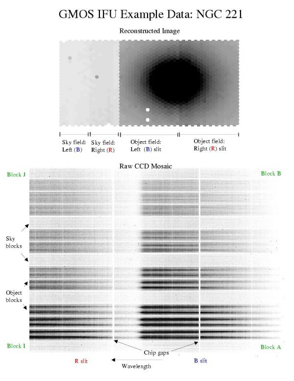
GMOS-N IFU Field-to-slit mapping
The relationship between the IFU fields and the layout on the detector for the GMOS-N IFU is further demonstrated with some example data on NGC 221 (M32) below. These data were taken in two-slit mode using the B600 grating, the g filter, and a central wavelength of 475 nm. The obvious step between the halves of the object field is a known flat-field effect (the R slit has higher average throughput than than the B slit) that can be corrected. It was left in for this example so that the halves could be distinguished more easily.
Performance
The throughput of the GMOS-N IFU has been measured by comparing the total flux in a GCAL imaging flat at the positions of the IFU fields with the flux through the IFU with no disperser in the beam. The throughputs for different wavelength are shown in the table below. The fiber-to-fiber variation in the throughput is about 6% for spectra in the center of the CCD and there is a ~30% reduction in throughput near the ends of the slits due to vignetting. Currently the flat-fielding is good to about 5%, varying between 3% and 10% depending on the slit block. The method is still being improved.
| Filter | Throughput |
| g | 62% |
| r | 65% |
| i | 62% |
| z | 58% |
Sensitivity estimates can be found on the GMOS Spectroscopic Sensitivity page which were derived using the GMOS Integration Time Calculator (ITC). The ITC reports results for single IFU elements.
Arc lines have Gaussian FWHM of about 4.2 pixels (unbinned). Thus, the effective slit width of the IFU in the dispersion direction is 0.31 arcsec.
Sky subtraction is done by averaging all spectra in a specified sky area (all the fibers in the "Sky" field, for example) and then subtracting the mean sky spectrum from all spectra in the cube. It is working well, though there can be gradients in the residuals with wavelength on the order of 5% (see figure below). Sky subtraction is sensitive to the flat-fielding accuracy, so it should improve as the flat-fielding improves.
Nod & Shuffle
The GMOS Nod & Shuffle mode applies techniques adopted for the infrared to optical MOS, long-slit, and IFU (Gemini-South only) spectroscopy whereby the sky is sampled with the same pixels used to observe the science target.
The advantages of observing with Nod & Shuffle include:
- Improved sky subtraction
- Potential increased density of slits
Disadvantages of observing with Nod & Shuffle include:
- Increased observing overheads
- Potential decreased field of view
Further details about Nod & Shuffle mode provided in this section are as follows.
- Basic concepts
- Band and micro shuffling
- Nodding
- Defining a Nod & Shuffle Observation
- Observing Strategies
- Focal plane masks
- Commissioning team
Basic Concepts
The capability of GMOS on Gemini to perform Nod & Shuffle operations is not one of the observing modes for which the instrument was originally designed and developed. The capability was proposed, developed, implemented and tested as an enhancement to the existing GMOS-N instrument from late 2001 to September 2002 by the GMOS Nod & Shuffle Commissioning Team. Below we give a brief overview of the Nod & Shuffle concept - for more information please see "Microslit Nod-Shuffle Spectroscopy: A Technique for Achieving Very High Densities of Spectra", Karl Glazebrook and Joss Bland-Hawthorn, 2001, PASP, 113, 197.
Nod & Shuffle allows the accurate subtraction of night sky emission by frequently nodding the telescope pointing between an object position and a sky position while simultaneously shuffling the charge on the CCD detectors between science and storage (unilluminated) regions. This is similar to the common practice in near-infrared astronomy of nodding or beam-switching, with the difference that the detector is not read out after each nod as is the case for background-limited near-infrared observations which do not suffer from read noise. The resulting image produced by the Nod & Shuffle technique contains two spectra obtained quasi-simultaneously through each slit in the focal plane mask - one of the object and one of the sky. Although these spectra are stored in different regions of the CCD detector, they were obtained with exactly the same pixels through identical optical paths. The effects of pixel response (flat-field), fringing, irregularities in the slit, and temporal variations in the sky cancel out when one subtracts the sky spectrum from the object spectrum. For long exposures, one can realize a factor of 10 improvement in the systematic uncertainties associated with subtraction of bright sky lines, especially in the red (600-1000 nm) where such errors typically dominate over photon or read noise. There is a trade-off, however: the noise in sky-subtracted Nod & Shuffle spectra is higher (by up to a factor of sqrt(2)) compared to classically sky-subtracted spectra using a very long slit. Thus Nod & Shuffle is not for every GMOS spectroscopy program.
Because with Nod & Shuffle one no longer derives the sky from regions adjacent to the object, one can use significantly shorter slits than in classical MOS spectroscopy which typically uses 5-10 arcsec long slitlets. In the limit where the slits have the same length as the object size (or the seeing disk), the density of these "microslits" can be 5-10 times higher than in the normal MOS mode. This can be particularly advantageous when performing MOS spectroscopy of crowded fields. However, because part of the detector is used for charge storage and therefore can not be illuminated, one necessarily loses between half and two-thirds of the GMOS field of view with Nod & Shuffle, depending on the Nod & Shuffle layout and shuffling mode selected. A further disadvantage of Nod & Shuffle observing is the increased overheads, described elsewhere.
The spectral images produced by Nod & Shuffle are, naturally, different from those produced by classical MOS spectroscopy and the data reduction is also different. Additional tasks to handle the reduction of Nod & Shuffle spectral data are included in the current releases of Gemini IRAF scripts, so these should not be considered a disadvantage.
Band- and Micro-shuffling
There are two shuffling modes that one can choose from when observing with Nod & Shuffle: band-shuffling and micro-shuffling. With band-shuffling the detector is divided into horizontal regions (or bands) of equal height which alternate between science and storage regions. Science regions are those areas of the detector which are allowed to be illuminated, and storage regions are never illuminated. Storage bands alternatively store science data when the sky spectra are being obtained and store sky data when the science spectra are being obtained. There must always be a storage band at the top and at the bottom of the detector. Science Bands can contain any number of slitlets of various slit-lengths. The limiting case where each science band contains exactly one slitlet and all slitlets have exactly the same slit-length is known as micro-shuffling.
Below we show three schematic layouts for Nod & Shuffle (click on each image for a larger view). The large, inset red square represents the GMOS imaging field of view (this is the area within which one is allowed to place slits in classical MOS observing). The science regions are shown as white with black filled rectangles representing the slits. The red and blue shaded regions represent storage regions. Normally the red shaded regions store the science data when the sky position is being observed, and the blue shaded regions store the sky data when the science target position is being observed. Because the sky and target are not observed simultaneously, the red and blue storage regions are allowed to overlap on the detector. These examples are not to scale and are for illustrative purposes only.
![[Single Band Shuffle]](/sciops/instruments/gmos/band-shuffle.gif) |
[a] The simplest possible layout is band-shuffling with a single science band. Here the middle third of the detector is the only science region, and the top and bottom thirds of the detector are used for storage exclusively. This band layout allows one to place a very high density of slits of variable length in a centralized region; however, one loses 2/3 of the field of view for slit placement. |
![[Two Band Shuffle]](/sciops/instruments/gmos/band-shuffle2.gif) |
[b] This example has two science bands and three storage bands. Because storage regions between science regions can be shared, one starts to win back field of view as the number of bands is increased. Here we are using 40% of the GMOS detector for science (available for slit placement) and 60% for charge storage. Once more each of the science bands can contain a high density and number of slits of variable length. Each band must have the same height and there must be two storage regions immediately adjacent to each science region; however, they do not need to be regularly spaced or fill the entire detector as shown here. This can be seen better in the next example. |
![[Micro Shuffle]](/sciops/instruments/gmos/micro-shuffle.gif) |
[c] The limiting case of many bands where each science region contains exactly one slit and, therefore, each slit has the same length. This special case is knows as micro-shuffling. As the number of micro-shuffled bands increases and the size of the slits decreases one can use nearly 50% of the GMOS field of view for slit placement. |
Nodding
When observing with Nod & Shuffle, one needs to define a nod vector and distance. This is the direction and the distance that the telescope will move when changing pointing from the object position to the sky position. In theory there is no restriction on the size and direction of the nod, though in practice there are several factors one should consider:
- How much additional overhead can the observations tolerate? Both the size and direction of the telescope nod will affect the amount of extra overhead incurred by the Nod & Shuffle observations compared to classical spectroscopic observations. While minimizing these extra overheads shouldn't be the primary consideration when selecting a telescope nod configuration, they can have an important impact on the observing efficiency.
- Does one wish to nod along the slit and observe the target in both the sky and object positions? This is a useful mechanism by which one can double the exposure time on the target and greatly reduce the overheads associated with Nod & Shuffle observing. However, this may not be possible or desirable for certain applications, e.g. observing crowded fields or extended objects. When nodding along the slit there are certain additional considerations to take into account when designing the Nod & Shuffle focal plane mask.
- If one is not nodding along the slit, one must define a sky position which does not place any objects in the slitlets. This can be tricky especially if one is using a large nod to a position for which deep imaging does not exist. It may be beneficial to request pre-imaging for both the target and sky positions if one anticipates using a very large (several arcmin) nod with Nod & Shuffle. Or perhaps more useful would be to request a short exposure (5min) at the sky position through the mask once it has been designed - this is the best way to make sure there are no bright objects contaminating the spectral image of the sky.
- Can one still guide in the sky position? For large nods (several arcmin or more) it is unlikely that the OIWFS will still be able to reach the guide star (the OIWFS patrol field is 3.54 arcmin x 4.15 arcmin). At this time, guiding with two separate guide stars in the target and sky positions is not a supported GMOS operational mode. It is still possible to take the sky spectra unguided (specify OIWFS in FREEZE mode for the sky position) but one must make doubly sure there are no bright objects that can wander into the slits during the unguided sky exposure. Note that observing with the sky position unguided will also help to reduce the Nod & Shuffle overheads.
- One is restricted to a single nod definition for each Nod & Shuffle observation. This means that the telescope will continuously nod between one target position and one sky position; this is known as the standard Nod & Shuffle mode. There are plans to support a pattern mode in a future implementation where the telescope nods between the target position and any number of user-specified sky positions in the same Nod & Shuffle observation.
Focal Plane Masks
Long Slits: Standard long-slits are available for Nod & Shuffle observing. These utilize the central third of the detector for science, the top and bottom thirds are used for charge storage. The longslits are listed on the GMOS long-slits page. Requests for long-slit configurations other than these will be handled as multi-object spectroscopy and the user must design the masks using the procedures described below.
Multi-Object Spectroscopy (MOS) Masks and the Maskmaking Software GMMPS: The mask-making software supports the design of Nod & Shuffle MOS Masks for both micro-shuffling and band shuffling. Details are available on the MOS pages.
Defining a N&S Observation
In this section we outline a few definitions and features of a GMOS Nod & Shuffle observation.
Cycle: A Nod & Shuffle cycle is defined as the smallest useful quantity in the Nod & Shuffle exposure. In theory, this is one exposure in the target position and one exposure in the sky position.
A = B: The exposure time in the target position during one cycle is defined as A. The exposure time in the sky position during one cycle is defined as B. For Nod & Shuffle observations with GMOS the exposure time A will always be equal to B.
A is even: Because of the slightly uneven performance of the GMOS blade-type shutter, Nod & Shuffle exposures are always taken in pairs in order to preserve photometry. Therefore, the exposure time A must be an even integer number of seconds.
B/2, A/2, A/2, B/2: In order to obtain the best sky subtraction, the sky exposure brackets the target exposure. Therefore, each Nod & Shuffle cycle with exposure time A is composed of 4 equal length sub-exposures taken in the following order - sky, object, object, sky.
Observation: A Nod & Shuffle observation is defined to have a set number of cycles, each with observing time A. Therefore, the total observing time (total open shutter time) for a Nod & Shuffle observation with a number of cycles C is equal to 2 × A × C.
Shuffle distance: The shuffle distance defines the height of the bands (or the length of the slits for micro-shuffling). Normally, the shuffle distance is a positive number, the sign determines whether the charge is shuffled up or down for the sky exposures. The object is always observed with the charge in the normal (no shuffling) configuration. For a positive shuffle, the resulting spectral images will have the sky spectrum located beneath the object spectrum with a separation equal to the shuffle distance. The shuffle distance is always specified in unbinned pixels, regardless of whether or not the spectral data is binned in the y-direction. For example, for a single-band Nod & Shuffle observation the shuffle distance is +1392 pixels for the Hamamatsu detector arrays at GS or GN (+1536 pixels for the previous e2v devices at GN); for a micro-shuffled image with 4 arcsec slits the shuffle distance is 50 pixels. If the spectral data is binned in the y-direction, one must make sure that the shuffle distance is a multiple of the binning (e.g., one cannot have a shuffle distance of 21 pixels if binning by 2 in the y-direction, but a shuffle distance of 20 or 22 pixels would be acceptable).
Charge traps:
Hamamatsu CCDs: charge traps are not an issue. It is no longer necessary to use these type of Darks with these detectors for charge traps removal.
E2V CCDs: The presence of local defects (charge traps) in GMOS detectors #2 and #3 lead to low-level horizontal stripes in Nod & Shuffle spectral images. There are two approaches to minimizing the effects of these defects. Since semester 2003B we have provided a special kind of dark exposure for Nod & Shuffle. Taking these dark exposures is very time consuming, and they are therefore only guaranteed to be made available for the following Nod & Shuffle configurations:
- A=60, 15 cycles, shuffle distance=31 pixels, CCD binned 2x1
- A=60, 15 cycles, shuffle distance=70 pixels, CCD binned 2x1
- A=60, 15 cycles, shuffle distance=1536, CCD binned 2x1
Any Nod & Shuffle darks defined by PIs in their Phase II proposals other than the above configurations will be taken on a best-effort basis. The Nod & Shuffle darks are effective for correcting for most of the effect of the defects. However, for very deep observations it is recommended to also translate the detector between Nod & Shuffle observations by ± a few pixels in the y-direction. This allows the defects to be removed in the data reduction stage via a suitable rejection algorithm. Nod & Shuffle programs that aim to go very deep should have their observations split into at least three dithered exposures. The translation of the detector must be defined by the PI in the OT using a GMOS sequence to change the DTA-X offset.
Baseline calibrations: For Nod & Shuffle programs all baseline calibrations are taken in exactly the same manner as for classical long-slit and MOS spectroscopy programs. Additional calibrations or calibrations taken in Nod & Shuffle mode must be requested explicitly in Phase I and Phase II proposals and Nod & Shuffle Darks must be defined by the PI in their Phase II OT program.
Sensitivity
Imaging
This page presents results from using the GMOS Integration Time Calculator (ITC). The table lists the estimated brightnesses of point sources and uniform surface brightness sources that give a signal-to-noise ratio (S/N) of 5 in a one-hour integration.
The ITC help pages include information on the filter zero points, calculation methods, and there is also information about guidelines and approximations specific to the ITC for GMOS.
The ITC includes adjustments for observing conditions in its calculations. For the table presented here, image quality was assumed to be 70%-ile and the other conditions were 50%-ile (median). Specifically, the estimates are for dark time and photometric conditions. The meanings of the observing condition criteria are explained in detail in the Observing Conditions pages. Further, an airmass of less than 1.2 was assumed. Those applying for time on Gemini should use the ITC to make calculations using the most flexible set of criteria possible, as the joint probability of all observing conditions being 50% percentile or better is only 6.2%.
All magnitudes listed below result in a S/N of 5 in a total integration time of 1 hour. The ITC calculates the S/N in an aperture that maximizes S/N given the predicted image quality for the observing conditions and wavelength requested. The sensitivity values in the table below use the optimum ITC aperture. For uniform surface brightness sources, an aperture with an area of 1 square arcsec is used. No binning of the detectors was used for these estimates.
The input magnitudes used for the ITC are in the passband given in the column "ITC standard passband". A spectrum of an A0V star was assumed.
The estimates assume that a 1 hour total exposure time was divided into 4 individual exposures in order to clean the images for bad pixels, cosmic-ray-events and to cover the areas in the gaps between the CCDs.
The sky subtraction aperture is assumed to be 5 times larger than the object aperture.
 This table was derived for GMOS North with the original e2v detectors. GMOS South gives similar results. The table was based on aluminum primary and secondary mirror coatings. Please use the appropriate integration time calculator for specific results (the ITC defaults to the current silver coatings).
| Filter | Central wavelength [nm] |
ITC standard passband |
Point Sources | Extended Sources | Exposure time |
| (mag) | (mag/arcsec2) | (sec) | |||
| g' | 475 | V | 26.5 | 27.0 | 4 x 900 |
| r' | 630 | R | 26.1 | 26.6 | 4 x 900 |
| i' | 780 | I | 25.5 | 25.9 | 4 x 900 |
| z' | 950 | I | 24.3 | 24.6 | 4 x 900 |
| Filter | Central wavelength [nm] |
ITC standard passband |
Point Sources [mag] |
Extended Sources [mag/arcsec2] |
Exposure time [sec] |
||
| BB (CCDb) | HSC(CCDg), SC (CCDr) | BB(CCDb) | HSC(CCDg), SC (CCDr) | ||||
| g' | 475 | V | 26.61 | 26.50 | 27.13 | 27.00 | 4 x 900 |
| r' | 630 | R | 26.27 | 26.20 | 26.67 | 26.60 | 4 x 900 |
| i' | 780 | I | 25.80 | 25.70 | 26.18 | 26.00 | 4 x 900 |
| Z | 875 | I | 24.94 | 24.80 | 25.28 | 25.20 | 4 x 900 |
| Y | 1010 | I | 23.32 | 23.20 | 23.62 | 23.50 | 4 x 900 |
This third table was derived for GMOS North as expected after the focal plane is upgraded to Hamamatsu CCDs. Sensitivities have been calculated for both the Hamamatsu Red and Blue CCD types; the single Hamamatsu Blue CCD covers the rightmost 1.37 arcmin x 5.5 arcmin portion of the imaging field of view. Note - the apparent slight improvement in g' and r' for the Hamamatsu Red CCDs is an artifact of the silver mirror coatings now assumed by the ITC, as the Hamamatsu Red and ev2 detectors for GMOS-N have essentially equivalent QE blueward of 650 nm.
| Filter | Central wavelength [nm] |
ITC standard passband |
Point Sources [mag] |
Extended Sources [mag/arcsec2] |
Exposure time [sec] |
||
| Hamamatsu Red | Hamamatsu Blue | Hamamatsu Red | Hamamatsu Blue | ||||
| g' | 475 | V | 26.59 | 26.72 | 27.04 | 27.17 | 4 x 900 |
| r' | 630 | R | 26.19 | 26.22 | 26.62 | 26.65 | 4 x 900 |
| i' | 780 | I | 25.76 | 25.74 | 26.16 | 26.15 | 4 x 900 |
| Z | 875 | I | 24.87 | 24.83 | 25.25 | 25.22 | 4 x 900 |
| Y | 1010 | I | 23.42 | 23.35 | 23.69 | 23.62 | 4 x 900 |
Spectroscopy
Brightnesses of point sources and extended sources giving signal-to-noise ratios (S/N) of 5 in a one-hour integration with GMOS are given in the table below. They were estimated using the GMOS Integration Time Calculator (ITC) and apply to the grating and filter combinations given in the table.
The ITC help pages include information on the filter zero points, calculation methods, and there is also information about guidelines and approximations specific to the ITC for GMOS.
The ITC includes adjustments for observing conditions in its calculations. For the table presented here, image quality was assumed to be 70%-ile and the other conditions were 50%-ile (median). Specifically, the estimates are for dark time and photometric conditions. The meanings of the observing condition criteria are explained in detail in the Observing Conditions pages. Further, an airmass of less than 1.2 was assumed. Those applying for time on Gemini should use the ITC to make calculations using the most flexible set of criteria possible, as the joint probability of all observing conditions being 50% percentile or better is only 6.2%.
All magnitudes listed below result in a S/N of 5 per (binned) pixel in the spectral direction in a total integration time of 1 hour, at the wavelengths given in the column "Wavelength". Spectral binning was chosen to give 3-4 pixels per resolution element. A spatial binning factor of 2 was used, which gives sufficient sampling for the median image quality. The ITC calculates the S/N in a spatial aperture that maximizes S/N given the predicted image quality for the observing conditions and wavelength requested. The sensitivity values in the table below use the optimum spatial aperture. For uniform surface brightness sources, an aperture with an area of 1 square arcsec is used.
The magnitudes used for the ITC are in the passband given in the column "ITC standard passband". A spectrum of an A0V star was assumed.
The estimates assume that a 1 hour total exposure time was divided into 4 individual exposures in order to clean the images for bad pixels and cosmic-ray-events.
The sky subtraction aperture is assumed to be 5 times larger than the object aperture. It is assumed that the GMOS slit length is sufficient to give derive the sky from the on-source exposures.
The long-pass filters GG455 and OG515 may be used to eliminate 2nd order contamination for gratings B600_G5303 and R150_G5306. The table below shows the effect in throughput for R150_G5306 used with OG515. The SDSS filters g', r', i' and z' may be used to limit the spectral range and make it possible to use multiple "banks" of slit-lets in MOS mode. The table below shows the effect in throughput for R400_G5305 used with the r' filter.
This table was derived for the original GMOS-North EEV CCDs. GMOS-South EEV CCDs gave similar results (with the latter having slightly better sensitivity in the UV and blue). The table was based on aluminium primary and secondary mirror coatings. Please use the appropriate integration time calculator for specific results (the ITC defaults to the current silver coatings).
| Grating Filter |
ITC standard passband |
Wavelength (nm) | Binning (spectral x spatial) |
(Binned) Spectra pixel size (nm) |
Spectra resolution (nm) |
Slit width (arcsec) |
Point Sources | Extended Sources |
| (mag) | (mag/arcsec2) | |||||||
| R150_G5306 none |
R | 400 | 2 x 2 | 0.35 | 1.14 | 0.50 | 21.8 | 21.8 |
| 600 | 2 x 2 | 0.35 | 1.14 | 0.50 | 22.8 | 22.8 | ||
| 800 | 2 x 2 | 0.35 | 1.14 | 0.50 | 21.9 | 21.9 | ||
| 400 | 4 x 2 | 0.70 | 2.28 | 1.00 | 22.4 | 22.4 | ||
| 600 | 4 x 2 | 0.70 | 2.28 | 1.00 | 23.2 | 23.2 | ||
| 800 | 4 x 2 | 0.70 | 2.28 | 1.00 | 22.4 | 22.4 | ||
| R150_G5306 OG515_G0306 |
R | 600 | 2 x 2 | 0.35 | 1.14 | 0.50 | 22.7 | 22.7 |
| 800 | 2 x 2 | 0.35 | 1.14 | 0.50 | 21.7 | 21.7 | ||
| R400_G5305 none |
R | 600 | 1 x 2 | 0.085 | 0.40 | 0.50 | 21.4 | 21.4 |
| 800 | 1 x 2 | 0.085 | 0.40 | 0.50 | 20.8 | 20.8 | ||
| 600 | 2 x 2 | 0.17 | 0.80 | 1.00 | 22.1 | 22.1 | ||
| 800 | 2 x 2 | 0.17 | 0.80 | 1.00 | 21.5 | 21.5 | ||
| R400_G5305 r_G0303 |
R | 600 | 1 x 2 | 0.085 | 0.40 | 0.50 | 21.3 | 21.3 |
| B600_G5303 none |
R | 400 | 2 x 2 | 0.09 | 0.27 | 0.50 | 21.4 | 21.4 |
| 500 | 2 x 2 | 0.09 | 0.27 | 0.50 | 22.2 | 22.2 | ||
| 600 | 2 x 2 | 0.09 | 0.27 | 0.50 | 21.8 | 21.8 | ||
| 400 | 4 x 2 | 0.18 | 0.54 | 1.00 | 22.1 | 22.1 | ||
| 500 | 4 x 2 | 0.18 | 0.54 | 1.00 | 22.8 | 22.8 | ||
| 600 | 4 x 2 | 0.18 | 0.54 | 1.00 | 22.5 | 22.5 |
GMOS performance monitoring
- Measurement of throughput in imaging mode: observations required are imaging of photometric standards in (u)griz filters. Photometric weather is required, but observations can be performed during twilight. Observations for each filter are collected once a month.
- Measurement of throughput in spectroscopic mode: observations consist of spectroscopy of spectrophotometric standards with two gratings, one with peak response in the red (R150) and one in the blue (B600). Observations are taken using a 5'' slit at low airmass, to minimize the effects of differential refraction. The IFU mode as well as other gratings in long-slit mode can be calibrated through measurements of relative counts from flat-field exposures. Photometric weather required, but observations can be performed in twilight. Frequency is once every three months.
- Image Quality: Observations consist of images taken with guiding on, in good seeing conditions, at a range of elevations, with all filters. Exposure times have to be at least 30 seconds, in order to average out stochastic seeing variations. No dedicated observations are required for image quality monitoring---image quality is measured on images taken during normal science operations.
- Image fringing: Observations consist of seven dithered images obtained at relatively low airmass towards a blank field, in both i and z bands. Observations need to be guided, in order to make star removal easier. The OIWFS probe arm must not vignette the FOV in any dither position. Observations are collected once every six months.
- Detector cosmetics: Characterization and monitoring of detector artifacts, such as hot pixels and bad columns. Observations consist of dark exposures collected once a year.
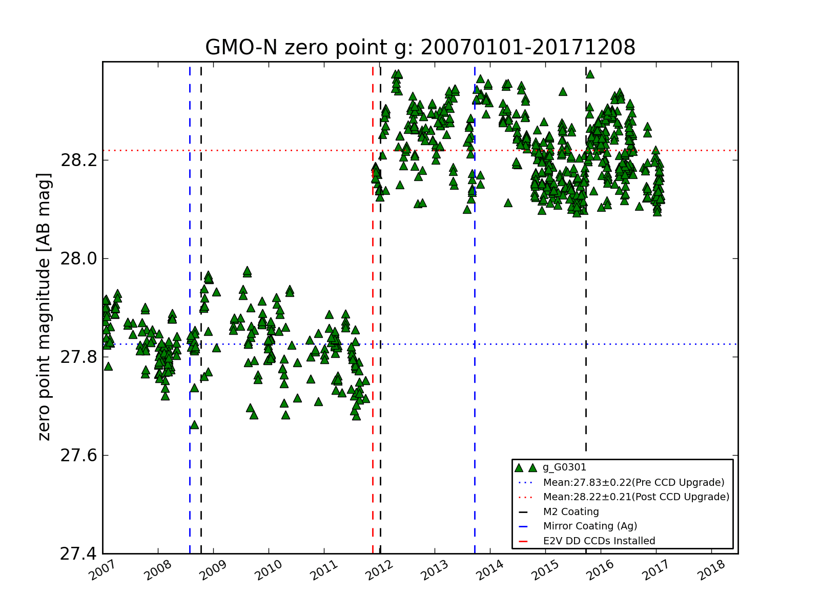
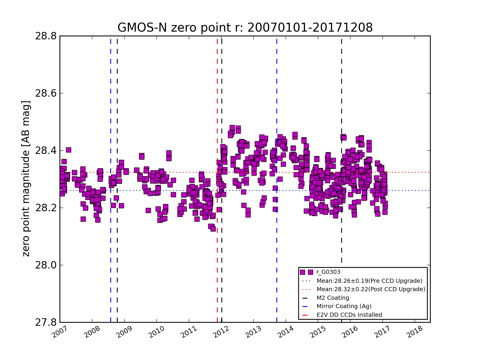
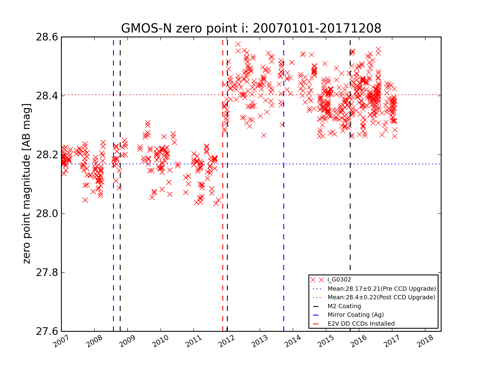
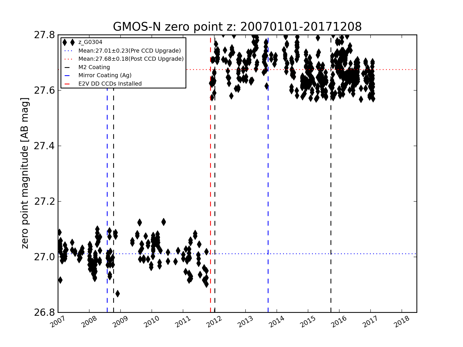
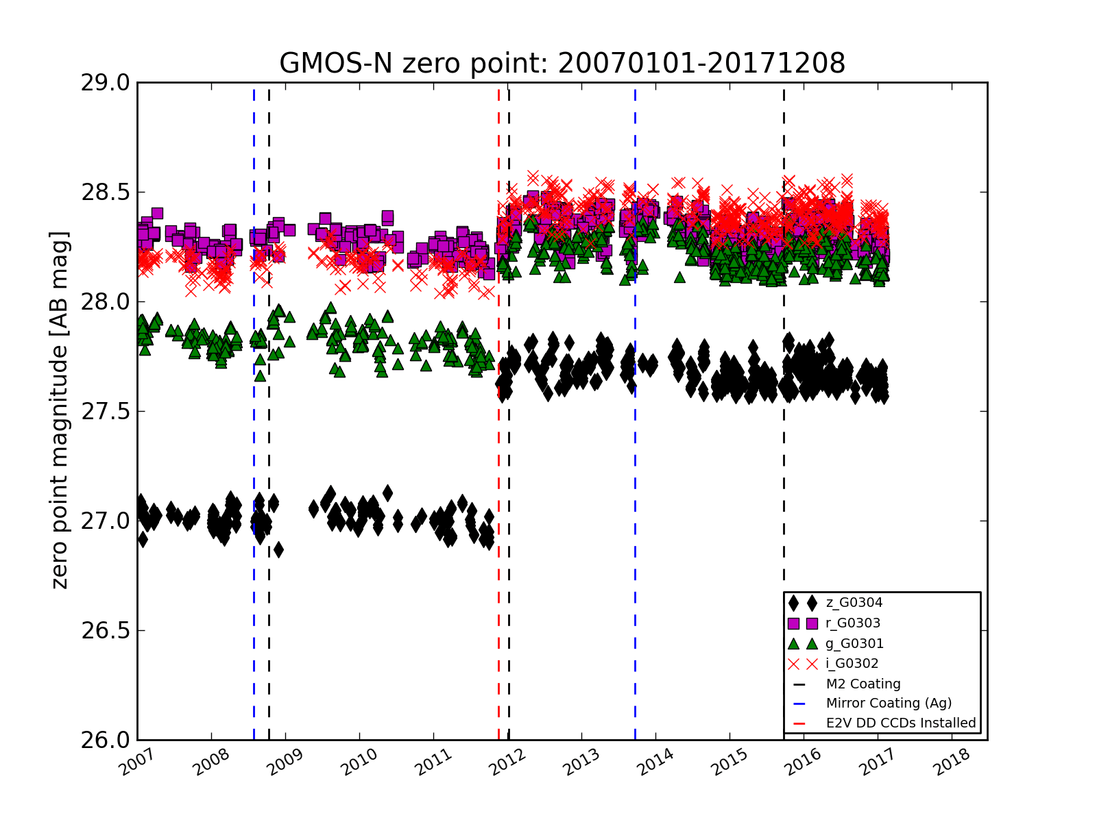
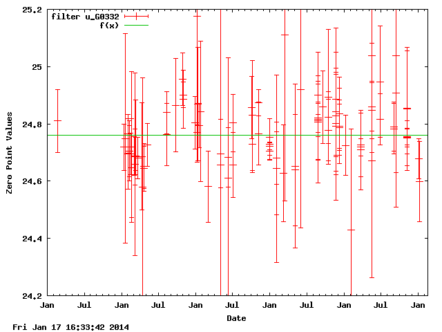
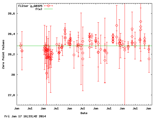
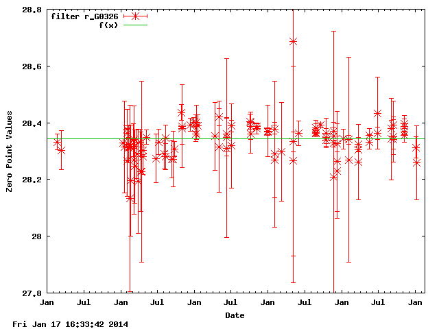
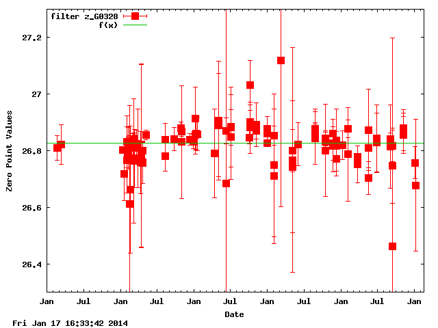
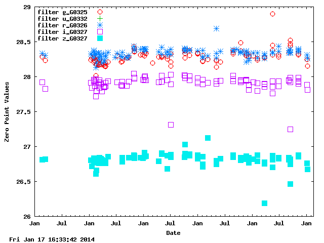
Photometric zero points
Imaging throughput is tabulated in the form of photometric zero points for griz bands for GMOS-N, and ugriz for GMOS-S. The AB zero-point magnitudes are given by:
mstd = mzero - 2.5 log (Ne/t) - k (μ -1),
where Ne is the background-subtracted number of electrons within the aperture, t is the exposure time, μ is the airmass, and CT is the color term coefficient. The AB magnitudes were measured within an aperture that is equal to 4 times the FWHM of the images, so they are insensitive to seeing variations. A detailed description of the data reduction procedures can be found in Jorgensen (2009). For other details, including information on standard fields adopted on both sites, please, consult the GMOS photometric standards page. Currently, zero points are only provided for CCD 2 and color terms are not being monitored. Further calibrations will be performed for the remaining CCDs and will be made available soon. For the data, follow the links below:
| Site | Band |
Individual Measurements |
Monthly Averages |
Plot |
| North | g | Table | Table | Click |
| North | r | Table | Table | Click |
| North | i | Table | Table | Click |
| North | z | Table | Table | Click |
| North | all | - | - | Click |
| South | u | Table | Table | Click |
| South | g | Table | Table | Click |
| South | r | Table | Table | Click |
| South | i | Table | Table | Click |
| South | z | Table | Table | Click |
| South | all | - | - | Click |
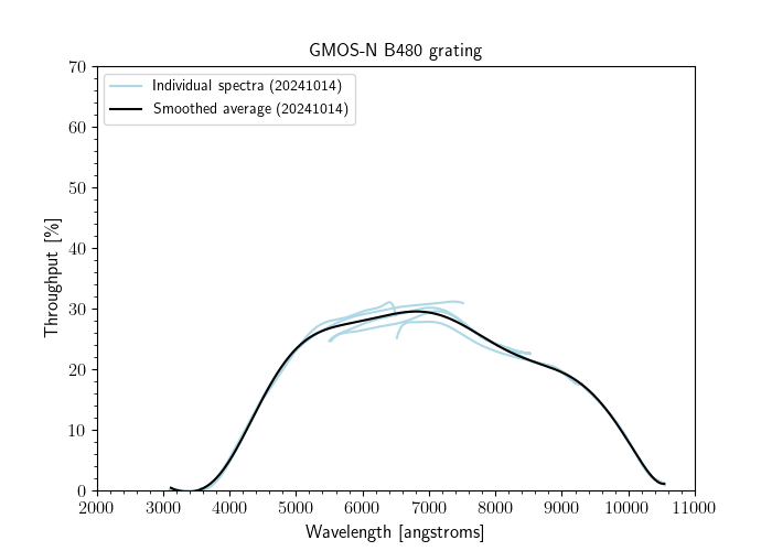
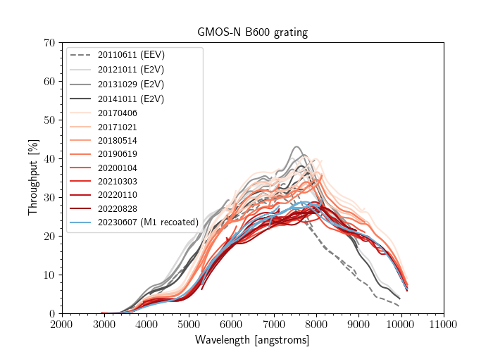
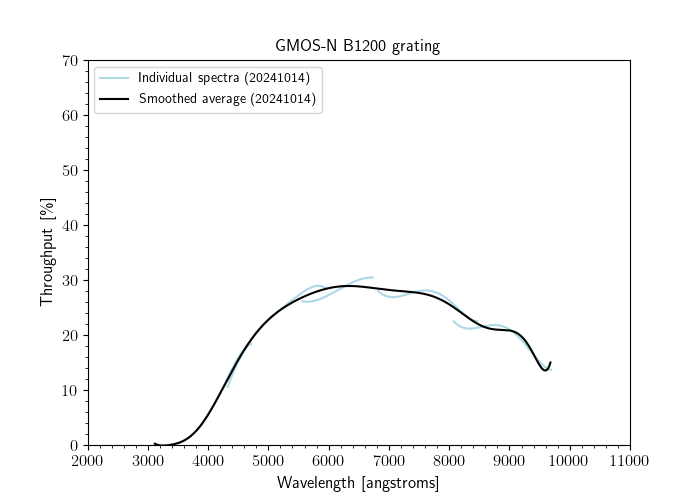
Spectroscopic Throughput
All throughput measurements are based on observations of spectrophotometric standards, collected under photometric conditions. Throughputs are defined as follows:
| T(λ) = | Nd(λ)
Nt (λ) |
where: Nd(λ) is the number of photons detected with wavelength λ and Nt(λ) is the number of photons of the same wavelength hitting the telescope's primary mirror. The latter is given by:
| Nt(λ) = N*(λ) 10 (-0.4 μ Aλ) |
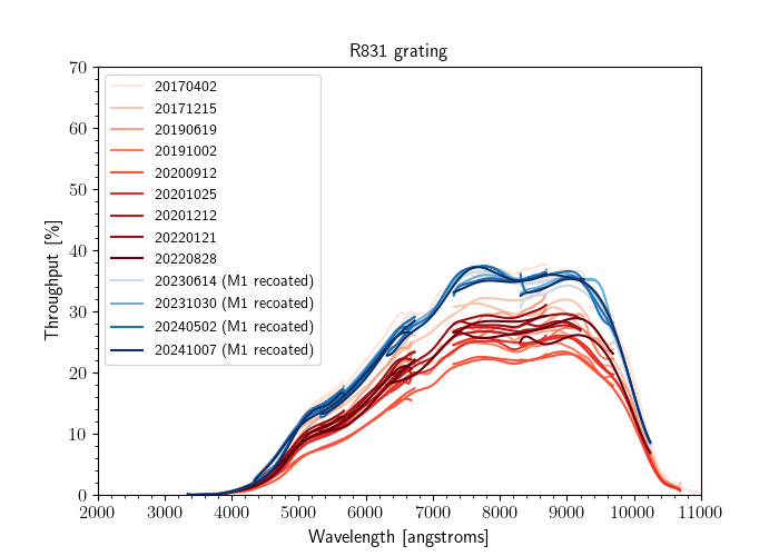
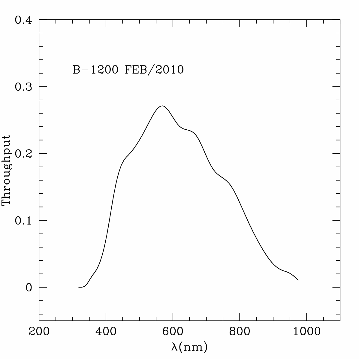
where N*(λ) is the star's photon flux at wavelength λ above Earth's atmosphere, in number of photons/cm2/s, μ is the airmass, and Aλ is a mean monochromatic extinction coefficient. For GMOS-N, extinction curves from Boulade et al. (1987, CFHT Bulletin 17, p.13) are used for λ < 400 nm, and from the CFHT users manual for longer wavelengths (numbers can be founds here). For GMOS-S, CTIO spectrophotometric extinction from Stone & Baldwin (1983 MNRAS, 204, 347) and Baldwin & Stone (1984 MNRAS, 206, 241) was adopted. The numbers available below are average values, that do not account for throughput variations as a function of grating angle.
| Site | Grating | Latest throughput | Plot | Time evolution |
| GMOS-N | B480 | 2024B | Click | Click |
| GMOS-N | B600 | not currently offered | N/A | Click |
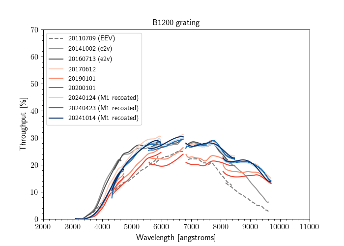
| GMOS-N | B1200 | 2024B | Click | Click |
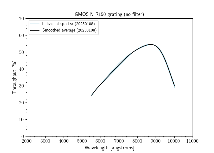
| GMOS-N | R150 | 2024B | Click | Click |
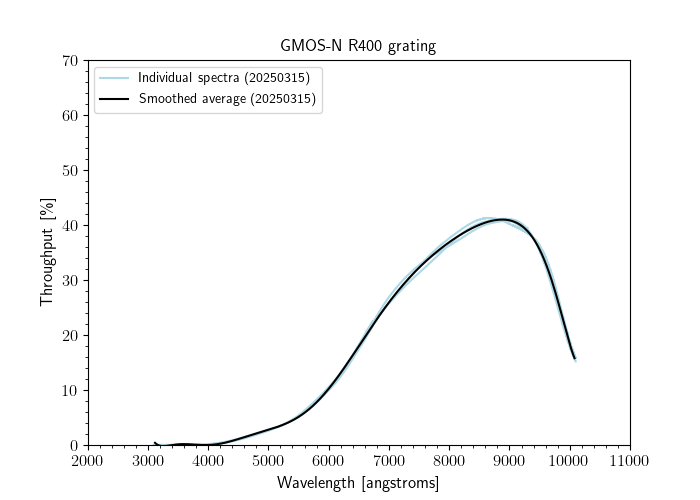
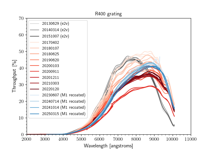
| GMOS-N | R400 | 2025A | Click | Click |
| GMOS-N | R600 | not regularly monitored | N/A | N/A |
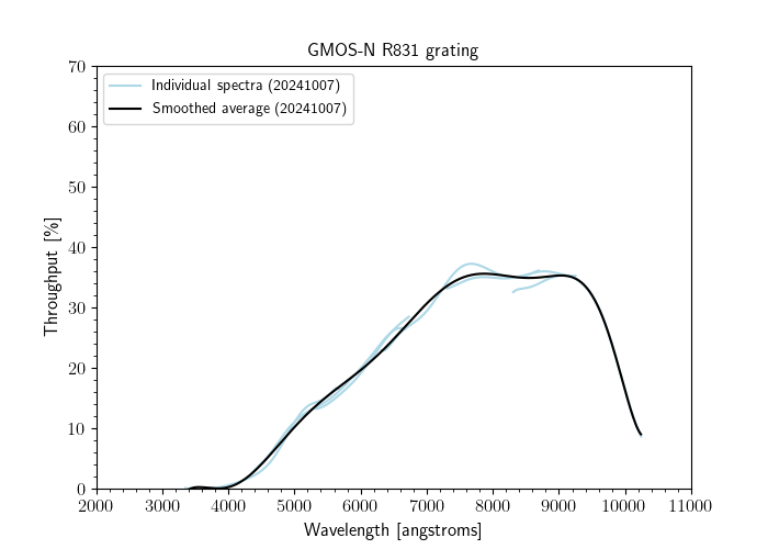
| GMOS-N | R831 | 2024B | Click | Click |
| GMOS-S | B600 | 2024A | Click | TBD |
| GMOS-S | B1200 | TBD | TBD | TBD |
| GMOS-S | R150 | 2024A | Click | TBD |
| GMOS-S | R400 | 2024A | Click | TBD |
| GMOS-S | B480 | 2024A | Click | TBD |
| GMOS-S | R831 | 2024A | Click | TBD |
.png)
| GMOS-S | All gratings throughput 2024 | Click |
Guiding Options
Two guiding options are available: the GMOS On-Instrument Wavefront Sensor (OIWFS) and the telescope's Peripheral Wavefront Sensors (PWFSs). It is strongly recommended that the GMOS OIWFS be used for all but non-sidereal objects. This is because (1) the PWFSs vignette a large part of the GMOS science field and (2) there is significant flexure between GMOS and the PWFSs.
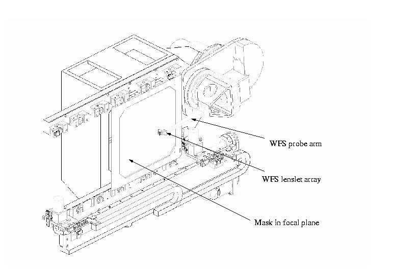
GMOS OIWFS
The GMOS On-Instrument Wavefront Sensor (OIWFS) consists of a 2x2 lenslet array on a moveable arm that patrols an area in front of the mask plane. Signals from the OIWFS are fed to the secondary for fast tip-tilt guiding.
- Filter: GG495 (longpass filter with a blue cut-off at 495nm)
- Limiting magnitude and availability of guide stars: Guide stars for the OIWFS need to be fainter than V=9.5mag. Limiting magnitude measurements for the OIWFS have been made in photometric, low wind conditions, and are summarized in the tables below. An unexpected difference in performance between the GMOS-N and GMOS-S OIWFSs exists, presumably due to significantly higher noise on the GMOS-S OIWFS. Attempts to reduce the noise on the GMOS-S OIWFS are on-going; in the meantime PIs must ensure their guide stars are valid for the appropriate GMOS. Bear in mind that programs that can be carried out in non-photometric conditions require sufficiently bright guide stars to enable guiding through clouds.
The effective limiting magnitude for the OIWFS also depends on the seeing and the guide frequency. Fainter guide stars can be utilized if the guide frequency is lowered, but this will degrade the image quality and cannot be employed in high wind situations. - GMOS-N: It is required that guide stars be brighter than V=16 mag for guiding on dark sky (BG=50% or BG=20%) in seeing conditions of IQ=70% or IQ=20%. For guiding in moon light under the same seeing conditions (BG=Any), guide stars need to be brighter than V=15.0 mag. For programs that can be executed in poorer seeing conditions, guide stars that are 1-2 magnitudes brighter are needed. Users are encouraged to select guide stars as bright as possible.
GMOS-N OIWFS limiting (V) magnitudes Seeing Dark sky (BG=50% or BG=20%) Full moon (BG=Any) < 0.75arcsec (IQ=70% or IQ=20%) 200Hz 15.5 mag
100Hz 16.2 mag
50Hz 17.1 mag200Hz 15.0 mag
100Hz 15.3 mag
50Hz 15.5 mag1.5arcsec (IQ=Any) 200Hz 13.8 mag
100Hz 14.9 mag
50Hz 15.5 magEstimate
100Hz 13.0 mag - GMOS-S: It is required that the guide stars be brighter than V=15.5 mag for guiding on dark sky in seeing conditions of 70-percentile or better. For guiding in moon light under the same seeing conditions, guide stars need to be brighter than V=14.5 mag. For programs that can be executed in poorer seeing conditions, guide stars that are 1-2 magnitudes brighter are imperatively needed. Users are encouraged to select guide stars as bright as possible.
GMOS-S OIWFS limiting (V) magnitudes Seeing Dark sky Full moon < 0.75arcsec V < 15.5 mag V < 14.5 mag 1.5arcsec V < 15.0 mag V < 14.0 mag
REMARK: These GMOS-S limit numbers are usually attainable only at 50Hz, the lowest guiding frequency value. - Patrol field: 3.54 arcmin x 4.15 arcmin = = 14.7 sq arcmin, overlapping one corner of the imaging field with some area outside the imaging field. The patrol area is the red box on the schematic diagram below. The patrol area is effectively doubled since the field can be rotated 180 degrees. The OIWFS cannot patrol outside a circle (the green one in the diagram below) with radius 4.8 arcmin. Thus a small area in the lower right of the patrol area shown on the schematic cannot be reached.
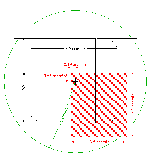
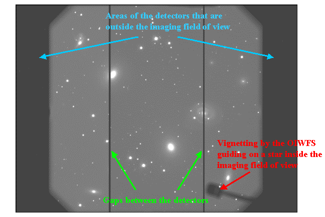
- Vignetting of GMOS science field by OIWFS: An image showing the vignetting of the GMOS science field by the OIWFS is shown below. The OIWFS on that image is in the center of the field, just for illustration. The OIWFS can be placed anywhere in the patrol field outlined on the diagram above, including outside the imaging field.
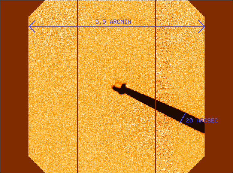
Vignetting of GMOS science field by OIWFS, if the OIWFS is in the center of the imaging field. The imaging field of view of 5.5 arcmin is shown. The width of the OIWFS arm as seen by the GMOS camera is about 20 arcsec.
| OIWFS detector parameters | |
| Array | EEV CCD-39 |
| Pixel format | 80x80 |
| Pixel size | 24 micron pixels |
| Spectral Response | 0.37 at 450nm, 0.70 at 700nm, 0.41 at 900nm |
| Readout time | 4.71ms for full frame |
| Readnoise | 3.05e-/pix |
| Total noise (on telescope during observations) | 5.95e-/pix |
| Dark current (uncooled) | 28.2 e-/s/unbinned pixel |
PWFS
The peripheral wavefront sensors (PWFS) vignette a large part of the GMOS science field. Furthermore, it has been found that there is significant flexure between GMOS and the PWFSs. At this time it is therefore recommended to use the on-instrument wavefront sensor for all GMOS observations with the exception of non-sidereal tracking, since the OIWFS implementation is purely electronic and limited to a small field of view.
At a later time when the flexure between the PWFSs and GMOS has been modeled and can be corrected, the PWFSs may be used for all spectroscopic observations (though the vignetting of the GMOS field of view may limit the usefulness for MOS). Until then, GMOS spectroscopy guided with the PWFSs are restricted to non-sidereal targets, or targets for which it is impossible to reach a guide star with the OIWFS. Depending on the slit width, reacquisitions may be required every ~45 minutes as the target drifts off the slit due to flexure. The target is less likely to drift completely out of the IFU, though re-centering the target every 45 minutes is potentially still necessary. PIs should assume an additional 6 minutes of reacquisition time for every 45 minutes of GMOS spectroscopy when guiding with the PWFSs.
Care must be taken to select guide stars such that the slit or IFU is not vignetted. An example of a set-up for long-slit spectroscopy is shown below.
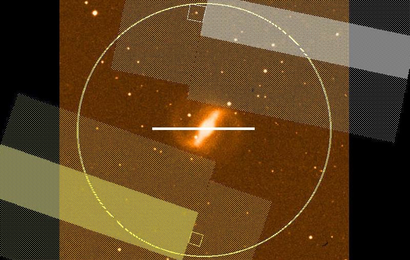
Schematic diagram showing the vignetting caused by the PWFSs. In this example the circle corresponds to the 7 arcmin outer radius of the PWFS patrol area. The white horizontal line in the center shows a GMOS long-slit. The large, shaded irregular boxes are the vignetting patterns of the two PWFSs; PWFS1 in the top of the image and PWFS2 in the bottom of the image. PWFS2 is not positioned on a star.