Announcements
Detector Array
Detector characteristics are given in this section. Note that the GMOS-South and GMOS-North detectors have been upgraded to Hamamatsu CCDs in 14B and 17A, respectively. Note also that the telescope optics are currently silver-coated, reducing the system throughput in the blue.
The GMOS-S detectors were upgraded to the new Hamamatsu CCDs in June/July 2014, improving red sensitivity, and including an upgraded detector controller. The GMOS-North original EEV detectors were replaced with e2v deep depletion devices in October 2011, improving sensitivity in the blue and greatly improving / extending sensitivity to longer wavelengths. A new focal plane array populated with Hamamatsu devices was installed in GMOS-N in February/March 2017, so that both GMOS instruments are currently operated with Hamamatsu devices.
For updates on status of the GMOS-N and GMOS-S detector arrays, see the Status and Availability webpage. Additional information on the current GMOS-N detector status is available here.
For the Hamamatsu detectors, the default detector read-out configuration is
- slow read
- low gain
- 12 amplifiers
The six-amplifier mode is not supported (three-amplifier mode is not available for these CCDs). Fast read-out speed is available for time resolved observations and high gain for observations of very bright objects.
For the e2v DD detectors used in GMOS-N until February 2017, the recommended detector read-out configuration was
- slow read
- low gain
- 6 amplifiers
The original intent for the e2v DD detectors was to use the three best amplifiers, giving the lowest read-noise. (This was the case for the original EEV detectors.) However, a recabling enacted to reduce spurious noise yielded the 3 amplifiers mode unavailable, so that all GMOS-N data taken with the e2v DD detectors utilized 6-amp mode.
- New GMOS-North Array Characteristics (Hamamatsu)
- GMOS-N Hamamatsu Array Current Status (Updated March 2022)
- GMOS-North Array Characteristics (e2v DD)
- GMOS-North Array Gain and Read Noise (e2v DD)
- Old GMOS-North Array Characteristics (EEV)
- Old GMOS-North Array Gain and Read Noise (EEV)
- New GMOS-South Array Characteristics (Hamamatsu)
- GMOS-South Array Characteristics (E2V)
- GMOS-South Array Gain and Read Noise (Hamamatsu)
- GMOS-South Array Gain and Read Noise (Older)
GMOS-N Hamamatsu Array
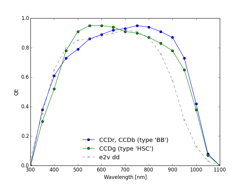
The upgraded GMOS-N detector array consists of three ~ 2048 x 4176 Hamamatsu chips of two different types arranged in a row. The central CCD (CCDg) has an enhanced response between ~450 and 650 nm compared to the left- and right-most CCDs (CCDr and CCDb, which probe the red and blue end of the spectral dispersion). CCDr and CCDb are both of the same type and have an enhanced response below ~450 nm and above ~650 nm. In the ITC, the central CCD is referred to as "HSC", while the two outer CCDs are referred to as "BB". The Hamamatsu detector array has the same orientation as the previous e2v deep depletion array and continues to support Nod-and-Shuffle mode. The expected QE of the GMOS-N Hamamatsu CCDs compared to the previous e2v deep depletion devices is shown in the plot below. See the Status and Availability webpage for more details.
First results from the commissioning of the GMOS-N Hamamatsu detectors were presented as a poster at the AAS summer meeting 2017 in Austin, Texas:
![[First results from the commissioning of the GMOS-N Hamamatsu detectors]](/sciops/instruments/gmos/Poster_GMOSN_Ham_AAS17.png)
The table below summarizes some of the Hamamatsu detector/controller characteristics
| Array | Hamamatsu | ||
| Pixel format | 6278 x 4176 pixels (mosaiced) | ||
| Array layout | Three 2048 x 4176 chips in a row with 67 pix = 1.005 mm gaps(*) | ||
| Pixel size | 15 microns square; 0.0807 arcsec/pixel | ||
| Spectral Response | approx 0.36 to 1.03 microns | ||
| Bias level | Bias Image | ||
| Flat field response | Example flat | ||
| Readout time | 1x1: characterization ongoing 2x2: characterization ongoing | ||
| Chip | CCDr | CCDg | CCDb |
| Chip ref no. | BI13-20-4k-1 | BI12-09-4k-2 | BI13-18-4k-2 |
| Dark current | ~3 e-/hr/pix | ~3 e-/hr/pix | ~3 e-/hr/pix |
| Full Well | ~129000 e- | ~123000 e- | ~125000 e- |
| Fringing at 900nm | < 1% | ~ 2% | < 1% |
(*) Due to bright columns on either side of the chip gaps, the effective gap size, not usable for science, is 80 pix = 1.200 mm.
Read-noise and Gain Values
The table below gives gain/read-noise values for the GMOS-N Hamamatsu CCDs. The values are averaged over all 12 amps.
| Readout | Gain | Resulting average | |
| rate | level | Gain (e-/ADU) | noise (e- rms) |
| Slow | Low | 1.63 | 4.14 |
| Fast | Low | 1.96 | 6.27 |
| Fast | High | 5.11 | 8.69 |
Slow Read / Low Gain is the primary mode for science use. Fast Read / Low Gain may be of use, for example, with acquisition observations or for time resolved observations. Fast Read / High Gain is expected to be used primarily for very bright targets.
Linearity
The linearity is better than 99.5% up to the full well values given in the Table above. (In the standard slow/low readout mode, the limit of the analog-to-digital converter will be reached before the full well depth.)
Cosmic hit rate
The cosmic ray hit rate is higher on the Hamamatsu CCDs - about 2.6 times more pixels are affected by cosmic rays, as compared to the previous E2Vs. As for GMOS-S, it is recommended to keep individual exposure times <=1200 s.
Gain and Read Noise Values
The table below gives gain/read-noise values for the current GMOS-N Hamamatsu CCDs measured in May 2017. (The gain is given in electrons/ADU. Readnoise is given in electrons.)
Note: GMOS-N data obtained with the previous E2V dd devices should use the corresponding E2V dd gain/readnoise values.
| SDSU Gain number |
Normal Science mode (2) |
Acquisition mode (6) |
Bright target mode (5) |
|||||
| CCD |
Sci Ext |
Amp. name | Gain | Noise | Gain | Noise | Gain | Noise |
| 1 | 1 | BI13-20-4k-1,4 | 1.66 | 4.06 | 2.01 | 8.02 | 5.21 | 9.90 |
| 1 | 2 | BI13-20-4k-1,3 | 1.63 | 4.12 | 1.95 | 6.88 | 5.18 | 8.94 |
| 1 | 3 | BI13-20-4k-1,2 | 1.62 | 4.12 | 1.97 | 6.01 | 5.05 | 8.75 |
| 1 | 4 | BI13-20-4k-1,1 | 1.57 | 3.99 | 1.91 | 5.88 | 5.04 | 8.17 |
| 2 | 5 | BI12-09-4k-2,4 | 1.68 | 4.20 | 2.03 | 6.71 | 5.29 | 9.42 |
| 2 | 6 | BI12-09-4k-2,3 | 1.65 | 3.98 | 1.97 | 6.34 | 5.13 | 8.91 |
| 2 | 7 | BI12-09-4k-2,2 | 1.64 | 3.88 | 1.96 | 5.39 | 5.14 | 8.19 |
| 2 | 8 | BI12-09-4k-2,1 | 1.68 | 4.20 | 2.01 | 5.86 | 5.29 | 8.84 |
| 3 | 9 | BI13-18-4k-2,4 | 1.61 | 4.04 | 1.95 | 6.10 | 5.03 | 8.13 |
| 3 | 10 | BI13-18-4k-2,3 | 1.63 | 4.35 | 1.95 | 6.13 | 5.10 | 8.53 |
| 3 | 11 | BI13-18-4k-2,2 | 1.58 | 4.02 | 1.89 | 5.98 | 4.86 | 8.03 |
| 3 | 12 | BI13-18-4k-2,1 | 1.65 | 4.55 | 1.95 | 6.79 | 5.09 | 8.80 |
| Ave | 1.63 | 4.13 | 1.96 | 6.34 | 5.12 | 8.72 | ||
GMOS-N Hamamatsu Array Current Status
An uncontrolled warm-up of the GMOS-N detector on February 26, 2022 resulted in new hot columns, consisting of a narrow bright column on amplifier 5 and broader bright columns on amplifiers 7 and 12. The issue with the broad hot columns on amplifiers 7 and 12 was resolved by a full thermal cycle performed between March 2 and 3. However, the narrow hot column on amplifier 5 persists.
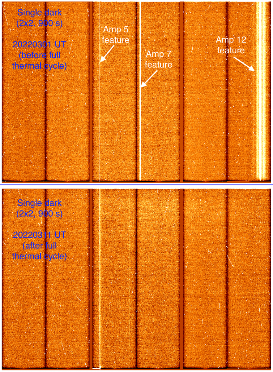
Overscan-subtracted darks showing the new GMOS-N hot columns after the uncontrolled warm-up and before the full thermal cycle (upper panel) and after the full thermal cycle (lower panel) which resolved the broad columns on amplifiers 7 and 12. (Since none of the frames has been bias-subtracted, the spatial bias structure is still visible.)
The persisting hot column on amplifier 5 saturates for typical science exposure lengths and results in saturation banding along amplifier 5 in binned data (a known effect around saturated stars for the GMOS-N detector in binned mode). The banding is imprinted on the overscan and subtracts out well during overscan subtraction.
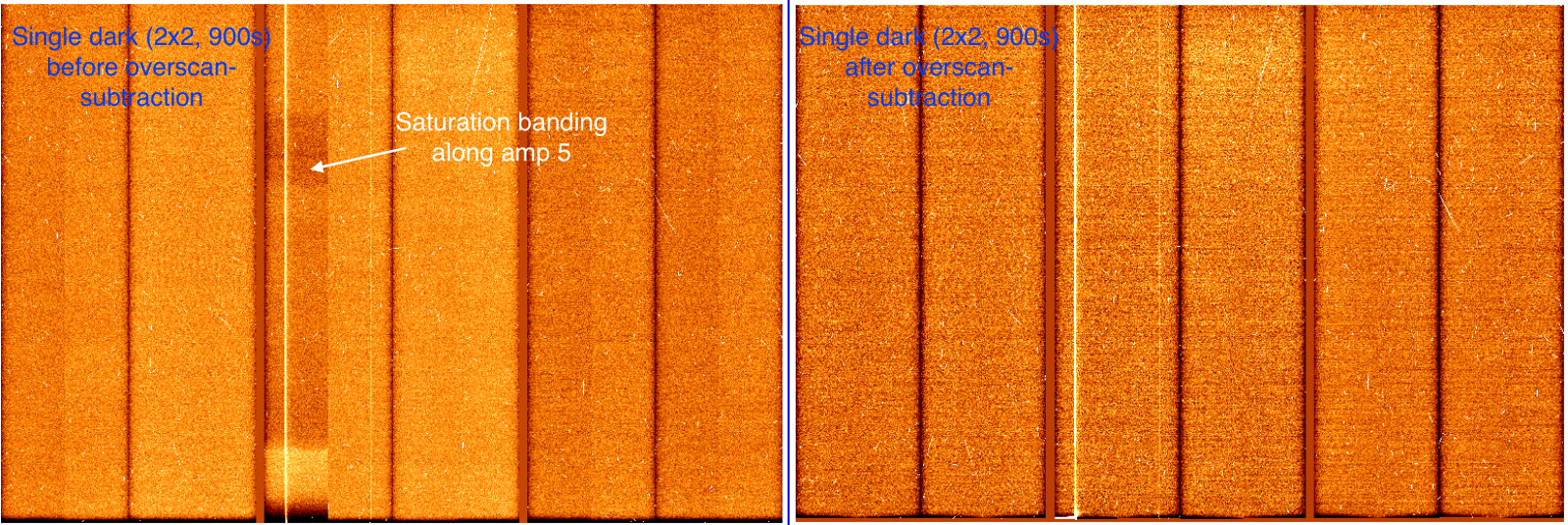
Single dark exposure before (left panel) and after (right panel) overscan-subtraction. The saturation banding cancels out well. (Since none of the frames has been bias-subtracted, the spatial bias structure is still visible.)
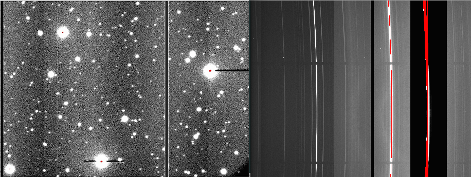
The saturated column on amplifier 5 shows a "bleeding" effect on the right side, causing an extended region of increased counts towards larger column numbers. In addition, a fainter mirrored image of the saturated column is seen on the neighboring amplifiers, primarily on amplifier 6 and, at a fainter levels, on amplifiers 4, 7, and 8.

Projection of the dark features after collapsing an overscan-subtracted 900 s dark (2x2 binning) along the detector rows (excluding the first 100 rows at the top and bottom, respectively). The projection is based on a median-average to remove cosmic rays. The arrows in the top panel mark the saturated column on amplifier 5 and its mirror images on amplifiers 4, 6, 7, and 8. The dark has not been bias-subtracted so that the underlying spatial structure highlights the chip gaps and amplifier limits. The lower panels show a magnification of the amplifier 5 feature and the most prominent mirror images on amplifiers 6 and 7. The bleeding of the amplifier 5 saturated column towards larger column number is evident from the lower left panel.
The following table provides the pixel location of the primary (saturated) amplifier 5 hot column (highlighted in red) and the fainter images of the column on neighboring amplifiers in mosaicked GMOS-N frames. Note that the center of the chip gap between CCD1 and CCD2 (i.e. amplifiers 4 and 5) is at pixel 2082 (1x1) and 1041 (2x2) in mosaicked images. If full spatial or spectral coverage is needed, dithers matching the separation between the chip gap and the amplifier 5 hot column should be avoided.
| Amplifier | Center pix (1 x 1) | Center pix (2 x 2) |
| 4 | 1881 | 941 |
| 5 | 2283 | 1143 |
| 6 | 2973 | 1486 |
| 7 | 3308 | 1655 |
| 8 | - | 1997 |
Bad pixel masks for the new hot columns will be provided as soon as they are available. Whether sky subtraction can mitigate the impact of the hot columns in spectroscopic data is currently being investigated. Updates will be posted on this webpage.
Summary of recommended observing strategies
Users of GMOS-N are advised to adjust their observing strategies to minimize the effect of the new hot column and its mirrored images on science data. The primary recommendations are:
- Placing targets (imaging) or spectral features of interest (spectroscopy) on the affected columns should be avoided as much as possible by choosing appropriate p offsets (imaging) or central wavelengths (spectroscopy).
- If full spectral coverage is needed (or avoiding the hot columns is impossible), an appropriate dither strategy should be used. A minimum dither of 5 pixels (binning 1 or 2) will cover the primary saturated part of the amplifier 5 hot column. Depending on the sensitivity requirements, a wider dither of 20 to 45 pixels should be considered to deal with the extended region affected by elevated counts around saturated column on amplifier 5. For imaging observations, the corresponding dithers need to be applied in the p direction. For spectroscopic observations, the dither size in wavelengths can be derived from the grating dispersion (nm/pixel) information in the GMOS grating table.
- Dither sizes matching the separation between the CCD1-to-CCD2 chip gap and the amplifier 5 hot column should be avoided if a continuous science coverage is needed. The separation between the center of the chip gap and the approximate center of the amplifier 5 hot column is ~200 pix in binning 1 and ~100 pix in binning 2. Note that some of the default dithers used to cover the inter-chip region (notably for the B1200 and R831 gratings) can cause overlap with the amplifier 5 hot column and should be revised accordingly.
Example arcs from the Gemini Observatory Archive can be used to derive the wavelength location of the hot columns based on the arc lines. This link shows an example search for GMOS-N arcs taken with the R400 grating in 2x2 binning with central wavelengths between 650 and 700 nm. Most wavelength setups should have archival arc lamp exposures with the Hamamatsu detector (i.e. data since March 2017) that can be used for comparison.
GMOS-S Array (Hamamatsu)
The upgraded GMOS-S detector array consists of three ~ 2048x4176 Hamamatsu chips arranged in a row. Two of the detectors (CCDr and CCDg) have an enhanced red response, these CCDs are referred to by the ITC as "Hamamatsu Red". The right-most CCD (CCDb, the blue end of spectral dispersion) in the focal plane array has improved blue response in addition to red response very similar to the Hamamatsu Red CCDs. This third CCD is referred to by the ITC as "Hamamatsu Blue". The orientation of the CCDs has not changed and continue to support the Nod and Shuffle observing mode. The plot below gives the anticipated QE comparison to the current E2V CCDs in GMOS-S. These QE plots are taken from general Hamamatsu information and lab measurements done in Hilo. See the Status and Availability webpage for more details.

The table below summarizes some of the Hamamatsu detector/controller characteristics (updated October 2015)
| Array | Hamamatsu | ||
| Pixel format | 6266x4176 pixels (mosaiced) | ||
| Array layout | Three 2048x4176 chips in a row with 61pix=0.915mm gaps | ||
| Pixel size | 15 microns square; 0.080 arcsec/pixel | ||
| Spectral Response | approx 0.36 to 1.03 microns [ Hamamatsu Red data / Hamamatsu Blue data / plot ] | ||
| Bias level | Bias Image | ||
| Flat field response | not yet available | ||
| Readout time | 1x1: 83sec(slow)/35sec(fast) 2x2: 24sec(slow)/11sec(fast) | ||
| Chip | CCDr | CCDg | CCDb |
| Chip ref no. | BI5-36-4k-2 | BI11-33-4k-1 | BI12-34-4k-1 |
| Dark current | ~ 3e-/hr/pix | ~ 3e-/hr/pix | ~ 3e-/hr/pix |
| Full Well | ~120,000 e- | ~122,000 e- | ~115,000 e- |
| Fringing at 900nm | <2% | <2% | <2% |
Readnoise and Gain Values (*)
The table below gives gain/read-noise values for the new GMOS Hamamatsu CCDs operating with the SDSU controller. The values are averaged over all 12 amps.
| Readout | Gain | Resulting average | |
| rate | level | Gain (e-/ADU) | noise (e- rms) |
| Slow | Low | 1.83 | 3.98 |
| Fast | Low | 1.57 | 6.57 |
| Fast | High | 5.20 | 7.86 |
The Slow Read / High Gain mode will not be offered for the Hamamatsu CCDs as it has been deemed to be of little scientific use. Slow Read / Low Gain is the primary mode for science use. Fast Read / Low Gain may be of use, for example, with acquisition observations or for time resolved observations. Fast Read / High Gain is expected to be used primarily for very bright targets.
(*) These values were updated after the installation of new video boards, and are valid for data taken from September 1, 2015 onwards. For data taken between July 2014 and August 2015, please look at the previous values.
Linearity
The linearity is better than 0.5% up to 60k ADU counts in these detectors, as measured from data taken during July-September 2014.
Cosmic hit rate
The cosmic ray hit rate is higher on the Hamamatsu CCDs - about 2.5 times more pixels are affected by cormic rays, as compared to the E2Vs.
Saturation banding in binned data (before september 2015)
The issue described below has been fixed as of August 31, 2015 and is currently no longer present.
This effect is a lowering in counts (with respect to the bias level) that happens when one or more pixels saturate, affecting the whole amplifier width. Examples are shown below, for imaging (left) and spectreoscopy (right). In the imaging example the "band" can be seen as it spans over the width of the corresponding amplifier. The counts within the "band" are lower (by a few hundreds) than the bias level (which is ~3000 ADU). For spectroscopy it looks more dramatic since it is a saturated arc line therefore the whole amplifier is 'lowered'. It does nor appear in 1x1 binning though.
The cause is understood (it is originated in the controller electronics, it is not a problem of the detector itself) and a fix implementation is currently (as of December 2014) under study; will probably be performed during 2015A (TBC)
Gain and Read Noise Values
The table below gives gain/read-noise values for the current GMOS Hamamatsu CCDs measured in September 2015, after the commissionig and characterization of the new video boards (see status and availability page for more details)
Note: GMOS South data obtained before Aug 31, 2015 should use the previous gain/read-noise values.
| SDSU Gain number |
Normal Science mode (2) |
Acquisition mode (6) |
Bright target mode (5) |
|||||
| CCD |
Sci Ext |
Amp. name | Gain | Noise | Gain | Noise | Gain | Noise |
| 1 | 1 | BI5-36-4k-2,4 | 1.834 | 4.04 | 1.556 | 5.49 | 5.183 | 8.07 |
| 1 | 2 | BI5-36-4k-2,3 | 1.874 | 4.28 | 1.593 | 6.35 | 5.300 | 8.85 |
| 1 | 3 | BI5-36-4k-2,2 | 1.878 | 4.24 | 1.592 | 7.10 | 5.330 | 9.13 |
| 1 | 4 | BI5-36-4k-2,1 | 1.852 | 4.21 | 1.566 | 6.68 | 5.240 | 8.93 |
| 2 | 5 | BI11-33-4k-1,4 | 1.908 | 3.90 | 1.634 | 5.77 | 5.407 | 8.02 |
| 2 | 6 | BI11-33-4k-1,3 | 1.933 | 4.24 | 1.648 | 7.38 | 5.459 | 8.62 |
| 2 | 7 | BI11-33-4k-1,2 | 1.840 | 4.07 | 1.582 | 6.14 | 5.225 | 8.59 |
| 2 | 8 | BI11-33-4k-1,1 | 1.878 | 4.29 | 1.613 | 5.19 | 5.334 | 8.35 |
| 3 | 9 | BI12-34-4k-1,4 | 1.813 | 4.15 | 1.549 | 7.72 | 5.120 | 9.34 |
| 3 | 10 | BI12-34-4k-1,3 | 1.724 | 3.61 | 1.478 | 7.88 | 4.894 | 7.99 |
| 3 | 11 | BI12-34-4k-1,2 | 1.761 | 3.72 | 1.545 | 6.80 | 5.129 | 8.30 |
| 3 | 12 | BI12-34-4k-1,1 | 1.652 | 3.53 | 1.445 | 6.36 | 4.828 | 7.94 |
| Ave | 1.829 | 3.96 | 1.567 | 6.57 | 5.204 | 5.86 | ||
Decommissioned detector Arrays
GMOS-N Array (e2v DD)
This interim upgrade GMOS-N detector array consists of three 2048x4608 chips arranged in a row. These e2v deep depletion (DD) detectors (device designation: 42-90 with multi-layer 3 coating) have enhanced blue and red response compared to the original EEV detectors, though these devices are not as sensitive in the red as the Hamamatsu detectors that will be installed in the near future. The fringing characteristics of the e2v DD devices is also much improved (<1% peak-to-peak expected) compared to the original EEV CCDs. Everything else (pixel scale, readout speed, image orientation, read noise, gain, full well) about these detectors is very similar to that of the original EEV devices. These devices were installed in mid-October 2011, and the first science data was collected with the new detectors November 22. See the Status and Availability webpage for more details.
The plot below gives the anticipated QE comparison to the current EEV CCDs in both GMOS-N and GMOS-S as well as to the eventual Hamamatsu SC and HSC devices. These QE plots are taken from general e2v information and will be updated with the QE curves supplied by the manufacturer when the CCDs are delivered.
![[GMOS CCDs QE Comparison]](/sciops/instruments/gmos/CCD_options.jpg "GMOS CCDs QE comparison. Click to view full image.")
Commissioning results for the e2v Deep Depletion CCDs were presented at the 2012 Winter AAS meeting in Austin, TX. Three poster presentations provided an overview and status report on both the e2v DD and Hamamatsu upgrade projects, results from on-sky commissioning and science data for the e2v DD CCDs, and results from daytime characterization data. These poster presentations are available for download as .pdf files below.
![[GMOS CCD upgrade project status]](/sciops/instruments/gmos/GMOS_poster1.gif "GMOS CCD upgrade project status. Click to view full image.")
![[GMOS-N e2v DD on-sky commissioning results]](/sciops/instruments/gmos/GMOS_poster2.gif "GMOS-N e2v DD on-sky commissioning results. Click to view full image.")
![[GMOS-N e2v DD daytime characterization results]](/sciops/instruments/gmos/GMOS_poster3.gif "GMOS-N e2v DD daytime characterization results. Click to view full image.")
The table below summarizes some of the e2v DD detector/controller characteristics.
| Array | e2v DD ML2AR CCD42-90-1-F43 | ||
| Pixel format | 6144x4608 pixels | ||
| Array layout | Three 2048x4608 chips in a row with ~ 0.5mm gaps | ||
| Pixel size | 13.5 microns square; 0.0728 arcsec/pixel | ||
| Spectral Response | approx 0.33 to 0.98 microns [ not yet available / plot ] | ||
| Bias level | Bias Image | ||
| Flat field response | not yet available | ||
| Readout time | See observing overheads page | ||
| Chip | CCD1 | CCD2 | CCD3 |
| Chip ref no. | 10031-23-05 | 10031-01-03 | 10031-18-04 |
| Dark current | n/a | n/a | n/a |
| Full Well (left / right) | 110.9 / 105.1 ke- | 115.5 / 108.9 ke- | 116.7 / 109.2 ke- |
| Fringing at 900nm | expected < 1% | expected < 1% | expected < 1% |
n/a values to be updated as detectors are characterized.
Readnoise and Gain Values
The table below gives average gain/read-noise values for the new GMOS e2v DD devices operating with the SDSU controller. The values are averaged over all 6 amps. The full table of read-noise and gain values at all settings and for all amps is available here.
The Slow Read / High Gain mode is not offered as it has been deemed to be of little scientific use. Slow Read / Low Gain is the primary mode for science use. Fast Read / Low Gain may be of use, for example, with acquisition observations or for time resolved observations. Fast Read / High Gain is expected to be used primarily for very bright targets.
<table border="1; bgcolor=" #ffffb7"="" align="center">
Readout Gain Resulting average rate level Gain (e-/ADU) noise (e- rms) Slow Low 2.27 3.32 Fast High 5.27 6.5 Fast Low 2.49 4.2
GMOS-N Gain & Read Noise (e2vDD)
The table below gives gain (e-/ADU conversion factors) and read-noise values for the GMOS-North e2v DD (deep depletion) CCDs installed in November 2011. High and low gain settings for the best amplifiers (3-amp mode) are highlighted for both slow and fast readout modes. Note: GMOS-North data obtained before November 1, 2011 should use the EEV gain/read-noise values.
| SDSU Gain number | 1 (High) | 2 (Low) | 5 (High) | 6 (Low) | ||||||
| CCD | Rate | Amp | Gain | Noise | Gain | Noise | Gain | Noise | Gain | Noise |
| 1 | F | L | 5.36* | 7.0* | 2.53* | 4.3* | ||||
| 1 | F | R | 5.34* | 7.8* | 2.53* | 4.2* | ||||
| 1 | S | L | n/a | n/a | 2.31 | 3.41 | ||||
| 1 | S | R | n/a | n/a | 2.31 | 3.17 | ||||
| 2 | F | L | 5.10* | 5.7* | 2.41* | 4.1* | ||||
| 2 | F | R | 5.27* | 5.8* | 2.50* | 4.1* | ||||
| 2 | S | L | n/a | n/a | 2.21 | 3.20 | ||||
| 2 | S | R | n/a | n/a | 2.27 | 3.22 | ||||
| 3 | F | L | 5.16* | 6.4* | 2.43* | 4.3* | ||||
| 3 | F | R | 5.41* | 6.3* | 2.56* | 4.4* | ||||
| 3 | S | L | n/a | n/a | 2.17 | 3.46 | ||||
| 3 | S | R | n/a | n/a | 2.33 | 3.44 | ||||
| Ave | F | 5.27* | 6.5* | 2.49* | 4.2* | |||||
| Ave | S | n/a | n/a | 2.27 | 3.32 | |||||
Rate: S=Slow (5µs dwell time), F=Fast (1µs dwell time)
*conversion factors estimated with ~ 5% uncertainty
GMOS-S Array (EEV)
This information refers to the EEV detectors at GMOS-S. These were removed in May 2014 and are no longer available. The Hamamatsu detectors were installed in June 2014.
The GMOS South detector array consists of three 2048x4608 EEV chips arranged in a row. The table below gives a summary of the current detector/controller characteristics.
| Array | EEV | ||
| Pixel format | 6144x4608 pixels | ||
| Array layout | Three 2048x4068 chips in a row with ~0.5mm gaps | ||
| Pixel size | 13.5 microns square; 0.073 arcsec/pixel | ||
| Spectral Response | approx 0.36 to 0.93 microns [ data / plot ] | ||
| Bias level | Bias image | ||
| Flat field response | Fringe images Flat field images | ||
| Readout time | See observing overheads page | ||
| Chip | CCD 01 | CCD 02 | CCD 03 |
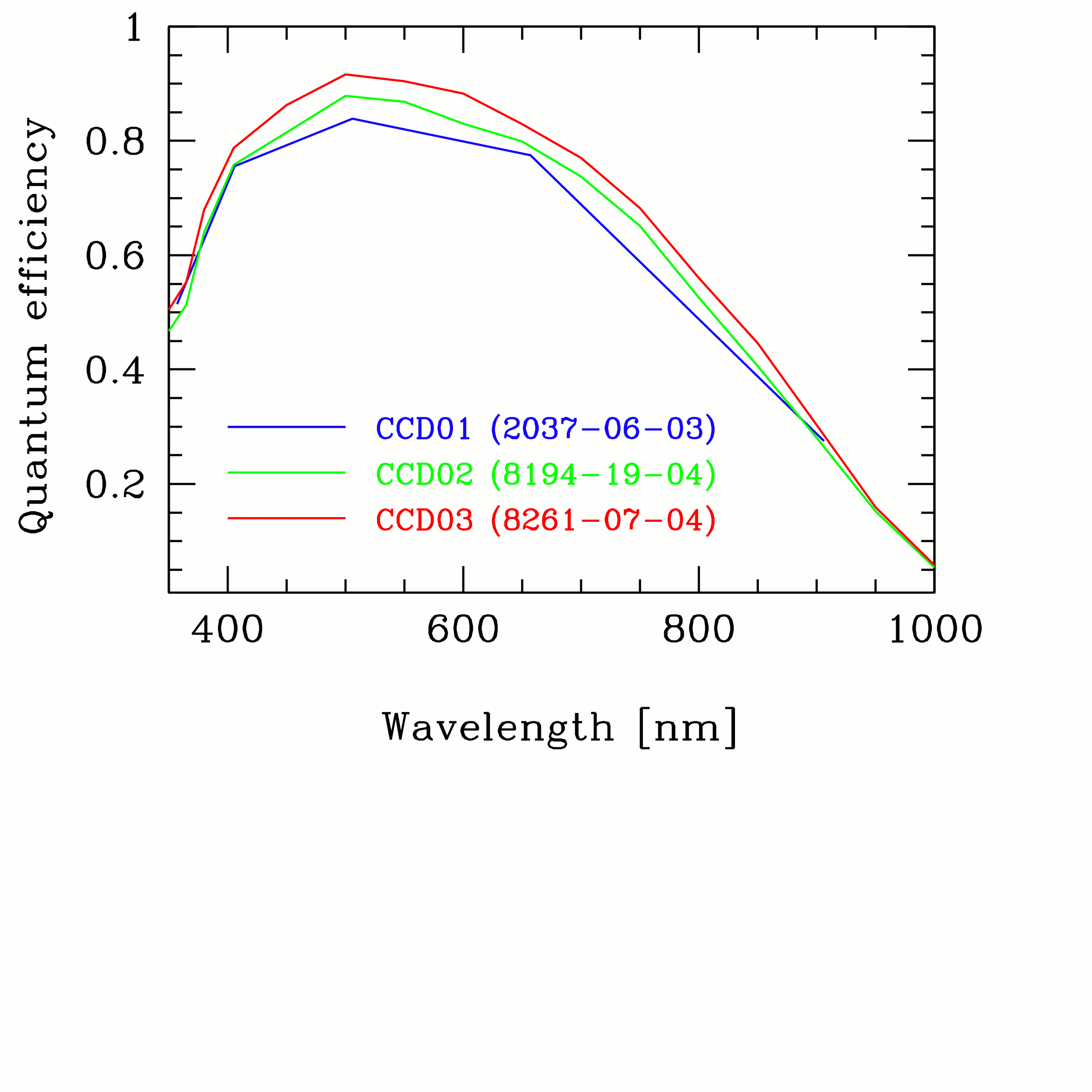
| Chip ref no. | EEV 2037-06-03 | EEV 8194-19-04 | EEV 8261-07-04 |
| Dark current* | 3 e-/pix/hr | 2 e-/pix/hr | 3 e-/pix/hr |
| Full Well ** | 125 ke- | 125 ke- | 125 ke- |
| Fringing at 900nm *** | 73% | 68% | 67% |
* Dark current measured at -113C by Gemini Observatory.
** Saturation can be avoided by assuming 100ke- for all chips
*** (peak-valley)/mean, measured from images taken at Gemini
Readnoise and Gain Values
The table below gives the gain/read-noise values for the GMOS EEV CCDs measured in September 2006 after a replacement of the video boards installed in the SDSU controller. Only the setting for the best amplifiers are listed (3-amp mode). The normal setting for science observations is slow read and low gain. For the full table of read-noise and gain values at all settings and for all amps, click here. Note: GMOS South data obtained before September 1, 2006 should use the previous gain/read-noise values.
| Readout | Gain | CCD 01 (left amp) | CCD 02 (left amp) | CCD 03 (right amp) | |||
| rate | level | Gain (e-/DN) | noise (e- rms) | Gain (e-/DN) | noise (e- rms) | Gain (e-/DN) | noise (e- rms) |
| Fast | High | 5.054 | 6.84 | 5.051 | 7.35 | 4.833 | 7.88 |
| " | Low | 2.408 | 4.49 | 2.295 | 4.42 | 2.260 | 4.09 |
| Slow | High | 4.954 | 5.70 | 4.532 | 4.81 | 4.411 | 4.34 |
| " | Low | 2.372 | 3.98 | 2.076 | 3.85 | 2.097 | 3.16 |
GMOS-N Array (EEV)
The original GMOS-N detector array consisted of three 2048x4608 EEV chips arranged in a row. This array was replaced by e2v deep depletion devices in October 2011.
The table below gives a summary of the original EEV detector/controller characteristics.
| Array | EEV | ||
| Pixel format | 6144x4608 pixels | ||
| Array layout | Three 2048x4608 chips in a row with ~0.5mm gaps | ||
| Pixel size | 13.5 microns square; 0.0727 arcsec/pixel | ||
| Spectral Response | approx 0.36 to 0.94 microns [ data / plot ] | ||
| Bias level | Bias image | ||
| Flat field response | Fringe images Flat field images | ||
| Readout time | See observing overheads page | ||
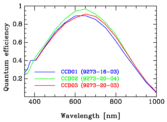
| Chip | CCD 01 | CCD 02 | CCD 03 |
| Chip ref no. | EEV 9273-16-03 | EEV 9273-20-04 | EEV 9273-20-03 |
| Dark current* | 0.8 e-/pix/hr | 0.7 e-/pix/hr | 0.5 e-/pix/hr |
| Full Well ** | 150 ke- | 101 ke- | 159 ke- |
| Fringing at 900nm *** | 29% | 19% | 24% |
* Dark current measured at -120C by NOAO
** Saturation can be avoided by assuming 100ke- for all chips
*** (peak-valley)/mean, measured from images taken at NOAO
Readnoise and Gain Values
The table below gives gain/read-noise values for the original GMOS-N EEV CCDs operating with the SDSU controller. Only the suggested settings are listed. The values are averaged over all 6 amps. For the full table of read-noise and gain values at all settings and for all amps, click here.
| Readout | Gain | Resulting average | |
| rate | level | Gain (e-/DN) | noise (e- rms) |
| Fast | High | 5.02 | 7.4 |
| " | Low | 2.49 | 4.9 |
| Slow | High | 4.40 | 4.8 |
| " | Low | 2.18 | 3.4 |
GMOS-N Gain & Read Noise (EEV)
The table below gives gain/readnoise values for the original GMOS-N EEV CCDs operating with the SDSU controller. Suggested high and low gain settings are highlighted for both slow and fast readout modes.
| sdsuGainSpeed [g,s] | 1,0 | 2,0 | 5,0 | 10,0 | 1,1 | 2,1 | 5,1 | 10,1 | ||||||||||
| Hardware Gain (g) | 1.0 | 2.1 | 4.8 | 9.5 | 1.0 | 2.1 | 4.8 | 9.5 | ||||||||||
| Integrator | 4.9 nf | 1.0 nf | ||||||||||||||||
| SDSU Gain number | 1 | 2 | 3 | 4 | 5 | 6 | 7 | 8 | ||||||||||
| CCD | Rate | Amp | Gain | Noise | Gain | Noise | Gain | Noise | Gain | Noise | Gain | Noise | Gain | Noise | Gain | Noise | Gain | Noise |
| CCD | Rate | Amp | Gain | Noise | Gain | Noise | Gain | Noise | Gain | Noise | Gain | Noise | Gain | Noise | Gain | Noise | Gain | Noise |
| 1 | F | L | 20.60 | 18.3 | 9.80 | 9.5 | 4.42 | 5.9 | 2.17 | 3.9 | 5.25 | 7.3 | 2.26 | 4.3 | 1.12 | 4.3 | 0.53 | 4.6 |
| 1 | F | R | 20.00 | 16.2 | 9.60 | 8.9 | 3.90 | 5.2 | 2.14 | 4.1 | 5.25 | 7.1 | 2.40 | 4.5 | 1.07 | 4.1 | 0.52 | 5.1 |
| 1 | S | L | 4.39 | 6.0 | 2.14 | 3.5 | 0.95 | 3.1 | 0.48 | 3.2 | 1.00 | 3.4 | 0.45 | 3.1 | 0.20 | 3.0 | 0.10 | 3.0 |
| 1 | S | R | 4.20 | 4.5 | 2.04 | 3.5 | 0.96 | 3.2 | 0.44 | 3.0 | 0.99 | 3.3 | 0.45 | 3.3 | 0.20 | 3.1 | 0.10 | 3.1 |
| 2 | F | L | 21.00 | 16.9 | 9.96 | 8.6 | 4.01 | 4.5 | 2.44 | 5.3 | 4.97 | 6.4 | 2.56 | 6.8 | 1.19 | 7.6 | 0.60 | 4.8 |
| 2 | F | R | 23.00 | 18.4 | 12.22 | 10.5 | 6.37 | 7.2 | 2.58 | 4.3 | 5.08 | 10.0 | 2.59 | 4.4 | 1.13 | 3.9 | 0.55 | 4.0 |
| 2 | S | L | 5.00 | 5.1 | 2.22 | 3.5 | 1.00 | 3.3 | 0.63 | 3.6 | 1.00 | 3.6 | 0.51 | 3.1 | 0.22 | 2.9 | 0.11 | 2.9 |
| 2 | S | R | 4.07 | 4.4 | 2.32 | 3.3 | 1.00 | 3.0 | 0.45 | 2.6 | 1.04 | 3.0 | 0.47 | 2.8 | 0.21 | 2.7 | 0.11 | 2.9 |
| 3 | F | L | 19.14 | 15.9 | 10.23 | 9.3 | 4.73 | 5.3 | 2.45 | 3.9 | 4.71 | 7.8 | 2.58 | 4.1 | 1.14 | 3.7 | 0.52 | 3.7 |
| 3 | F | R | 21.80 | 16.4 | 11.16 | 9.2 | 4.90 | 5.4 | 2.37 | 6.0 | 4.87 | 6.1 | 2.53 | 5.2 | 1.17 | 5.2 | 0.58 | 4.2 |
| 3 | S | L | 4.32 | 4.4 | 2.19 | 3.0 | 1.04 | 2.6 | 0.50 | 2.5 | 1.04 | 2.7 | 0.49 | 2.6 | 0.22 | 2.6 | 0.11 | 2.6 |
| 3 | S | R | 4.44 | 4.3 | 2.18 | 3.3 | 0.95 | 2.9 | 0.50 | 2.8 | 1.03 | 3.3 | 0.54 | 3.2 | 0.24 | 3.2 | 0.12 | 6.2 |
| Ave | F | 20.92 | 17.0 | 10.50 | 9.3 | 4.72 | 5.6 | 2.36 | 4.6 | 5.02 | 7.4 | 2.49 | 4.9 | 1.14 | 4.8 | 0.55 | 4.4 | |
| Ave | S | 4.40 | 4.8 | 2.18 | 3.4 | 0.98 | 3.0 | 0.50 | 3.0 | 1.02 | 3.2 | 0.48 | 3.0 | 0.21 | 2.9 | 0.11 | 3.4 | |
Rate: S=SLOW (5ns dwell time), F=Fast (1ns dwell time)
GMOS-S Gain & Read Noise (Old)
Hamamatsu detectors (June 2014 - Aug 31 2015)
The table below gives gain/read-noise values for the GMOS Hamamatsu CCDs before the replacement of the video C-boards by the improved E-boards that fixed the banding problem. Note: GMOS South data obtained with E2V detectors (i.e. before June 2014) should use the older values (see bottom)
| SDSU Gain number |
Normal Science mode (2) |
Acquisition mode (6) |
Bright target mode (5) |
|||||
| CCD |
Sci Ext |
Amp. name | Gain | Noise | Gain | Noise | Gain | Noise |
| 1 | 1 | BI5-36-4k-2,4 | 1.626 | 4.03 | 1.41 | 6.12 | 5.10 | 7.76 |
| 1 | 2 | BI5-36-4k-2,3 | 1.700 | 4.25 | 1.45 | 6.54 | 5.36 | 8.18 |
| 1 | 3 | BI5-36-4k-2,2 | 1.720 | 3.98 | 1.48 | 6.01 | 5.34 | 7.93 |
| 1 | 4 | BI5-36-4k-2,1 | 1.652 | 4.24 | 1.43 | 6.66 | 5.20 | 8.68 |
| 2 | 5 | BI11-33-4k-1,4 | 1.739 | 3.80 | 1.51 | 5.24 | 5.48 | 7.75 |
| 2 | 6 | BI11-33-4k-1,3 | 1.673 | 3.98 | 1.46 | 5.48 | 5.27 | 7.79 |
| 2 | 7 | BI11-33-4k-1,2 | 1.691 | 3.83 | 1.45 | 4.90 | 5.36 | 7.65 |
| 2 | 8 | BI11-33-4k-1,1 | 1.664 | 4.12 | 1.44 | 4.86 | 5.14 | 7.53 |
| 3 | 9 | BI12-34-4k-1,4 | 1.613 | 3.51 | 1.39 | 4.97 | 5.13 | 7.32 |
| 3 | 10 | BI12-34-4k-1,3 | 1.510 | 3.25 | 1.30 | 5.07 | 4.74 | 7.11 |
| 3 | 11 | BI12-34-4k-1,2 | 1.510 | 3.35 | 1.31 | 5.07 | 4.72 | 6.85 |
| 3 | 12 | BI12-34-4k-1,1 | 1.519 | 3.45 | 1.31 | 5.69 | 4.83 | 7.48 |
| Ave | 1.64 | 3.82 | 1.41 | 5.55 | 5.14 | 7.67 | ||
E2V detectors (Sep 1 2006 - May 19 2014)
The table below gives gain/read-noise values for the GMOS EEV CCDs measured in September 2006 after the replacement of the video boards installed in the SDSU controller. High and low gain settings for the best amplifiers (3-amp mode) are highlighted for both slow and fast readout modes. Note: GMOS South data obtained before September 1, 2006 should use the older values (see bottom)
| SDSU Gain number | 1 (High) | 2 (Low) | 5 (High) | 6 (Low) | ||||||
| CCD | Rate | Amp | Gain | Noise | Gain | Noise | Gain | Noise | Gain | Noise |
| 1 | F | L | 5.054 | 6.84 | 2.408 | 4.49 | ||||
| 1 | F | R | 5.253 | 6.54 | 2.551 | 5.07 | ||||
| 1 | S | L | 4.954 | 5.70 | 2.372 | 3.98 | ||||
| 1 | S | R | 4.862 | 5.19 | 2.403 | 4.01 | ||||
| 2 | F | L | 5.051 | 7.35 | 2.295 | 4.42 | ||||
| 2 | F | R | 4.954 | 11.37 | 2.288 | 5.03 | ||||
| 2 | S | L | 4.532 | 4.81 | 2.076 | 3.85 | ||||
| 2 | S | R | 4.592 | 4.96 | 2.131 | 3.83 | ||||
| 3 | F | L | 4.868 | 8.56 | 2.264 | 4.63 | ||||
| 3 | F | R | 4.833 | 7.88 | 2.260 | 4.09 | ||||
| 3 | S | L | 4.381 | 4.81 | 2.056 | 3.27 | ||||
| 3 | S | R | 4.411 | 4.34 | 2.097 | 3.16 | ||||
| Ave | F | 5.002 | 8.09 | 2.344 | 4.622 | |||||
| Ave | S | 4.622 | 4.968 | 2.189 | 3.683 | |||||
Rate: S=SLOW, F=Fast
-----
Older values (before September 1, 2006)
The table below gives the gain/readnoise values for the GMOS EEV CCDs operating with the SDSU controller. These values should be used to reduce GMOS South data obtained before September 1, 2006. High and low gain settings for the best amplifiers (3-amp mode) are highlighted for both slow and fast readout modes.
| SDSU Gain number | 1 (High) | 2 (Low) | 5 (High) | 6 (Low) | ||||||
| CCD | Rate | Amp | Gain | Noise | Gain | Noise | Gain | Noise | Gain | Noise |
| 1 | F | L | 5.29 | 6.33 | 2.51 | 4.94 | ||||
| 1 | F | R | 5.27 | 6.28 | 2.47 | 4.81 | ||||
| 1 | S | L | 4.92 | 5.13 | 2.33 | 3.97 | ||||
| 1 | S | R | 4.98 | 5.48 | 2.46 | 4.28 | ||||
| 2 | F | L | 5.03 | 6.14 | 2.32 | 4.73 | ||||
| 2 | F | R | 5.03 | 8.41 | 2.38 | 5.25 | ||||
| 2 | S | L | 4.38 | 4.69 | 2.07 | 3.69 | ||||
| 2 | S | R | 4.65 | 5.46 | 2.13 | 3.93 | ||||
| 3 | F | L | 4.88 | 6.92 | 2.32 | 4.99 | ||||
| 3 | F | R | 4.90 | 6.20 | 2.28 | 4.58 | ||||
| 3 | S | L | 4.43 | 4.85 | 2.08 | 3.65 | ||||
| 3 | S | R | 4.36 | 4.45 | 2.07 | 3.31 | ||||
| Ave | F | 5.07 | 6.71 | 2.38 | 4.88 | |||||
| Ave | S | 4.62 | 5.01 | 2.19 | 3.81 | |||||
Rate: S=SLOW, F=Fast
Last update October 02 2015: German Gimeno
Filters
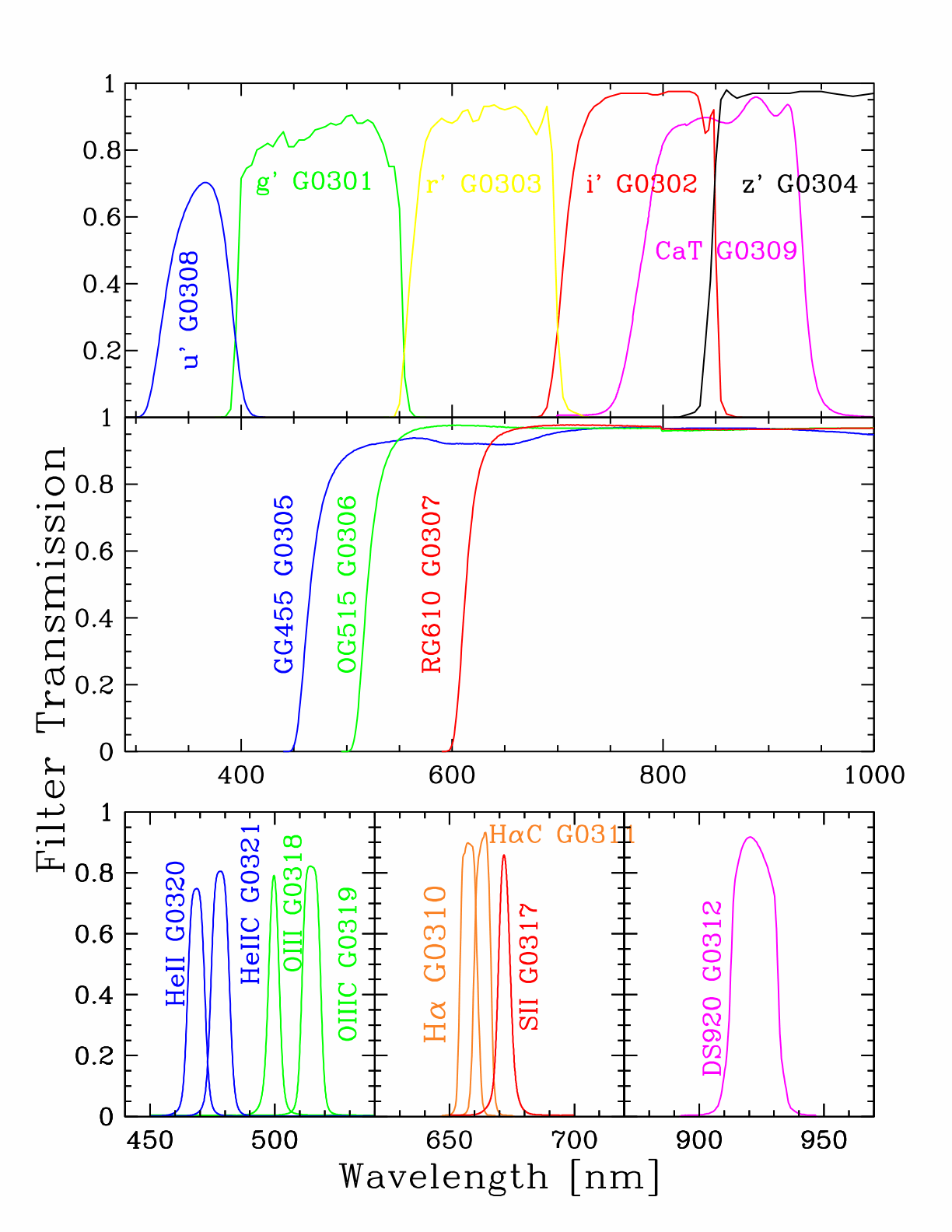
The GMOS filters u', g', r', i' and z' are similar to the filters used by the Sloan Digital Sky Survey (SDSS). A description of the SDSS photometric system is presented in Fukugita et al. (1996, AJ, 111, 1748). See the description of optical photometric standard stars for details on the photometric standard calibration.
Please note that due to filter degradation discovered in semester 2004A the u' filter is no longer available for science use on GMOS-N. It is also possible to install User-supplied filters in GMOS.
The filter CaT is a 150nm broad-band filter approximately centered on the Ca Triplet.
The Z and Y filters are similar to those installed in the United Kingdom Infra-Red Telescope (UKIRT) Wide Field Camera (WFCAM). A description of these filters is available from the UKIRT WFCAM user guide, see Table 1.1. The Z filter is designed to mimic the SDSS z' bandpass with red sensitive CCDs, while the Y filter occupies the clean wavelength range between the atmospheric absorption bands at 0.95µm and 1.14µm.
The ri (r+i) filter is a user-supplied filter available at GMOS-N, which covers the r and i bandpasses.
The filters Ha, HaC, OIII, OIIIC, SII, HeII, and HeIIC are narrow-band filters for H-alpha, H-alpha continuum, ionized oxygen, ionized oxygen continuum, ionized sulphur, ionized helium, and ionized helium continuum, respectively. The narrow-band OVI and OVIC filters are centered on the Raman 6835A OVI band and the nearby continuum.
The filter DS920 is a narrow-band filter centered on a wavelength region of very low sky background. This filter is only available with GMOS-N, and may be removed to make room for a u' filter.
The filters GG455, OG515, RG610 and RG780 are 5mm thick Schott glass filters. These are long-pass filters which can be used to block 2nd-order contamination of the spectra or limit the wavelength range to allow multiple slit-banks in the multi-aperture mode. The RG780 filter is only available with GMOS-S.
Transmission curves for each filter set based on lab measurements are available: GMOS-N filters and GMOS-S filters (The new Z and Y filters will be added once they have been characterized).
The table lists the properties of the filters based on laboratory measurements. The wavelength interval given in the tables is the interval within which the transmission is larger than 50 per cent. For the long-pass filters and the z' filters the wavelength at the 50 per cent transmission at short wavelength edge is given.
Some of the filters can be combined, the allowed combinations are listed last in the table. The combinations are useful for using the IFU in 2 slit mode with the higher dispersion gratings, e.g. R831 with the filter combination r' + RG610.
Imaging with GMOS requires use of either a color filter (griz, CaT, Z, Y) or a narrow band filter. The long-pass filters GG455, OG515, RG610, and RG780 are not suitable for imaging. Also imaging without a filter is not supported since neither GMOS is equipped with an Atmospheric Dispersion Corrector (ADC) at this time.
Users may supply their own filters for queue observations; see filter policy and specifications for details.
| GMOS Filters | ||||
| Filter | Filter number* [North / South] |
Effective wavelength [nm] |
Wavelength interval [nm] |
Transmission data [North / South] |
| Broad Band Imaging Filters | ||||
| u | G0308 (no longer available) |
350 | 336-385 | GMOS-N data |
| G0332 | GMOS-S data/plot | |||
| g | G0301 | 475 | 398-552 | GMOS-N data |
| G0325 | GMOS-S data/plot | |||
| r | G0303 | 630 | 562-698 | GMOS-N data |
| G0326 | GMOS-S data/plot | |||
| i | G0302 | 780 | 706-850 | GMOS-N data |
| G0327 | GMOS-S data/plot | |||
| CaT | G0309 | 860 | 780-933 | GMOS-N data |
| G0333 | GMOS-S data/plot | |||
| z | G0304 | >=925 | >=848 | GMOS-N data |
| G0328 | GMOS-S data/plot | |||
| Z | G0322 | 876 | 830-925 | WFCAM Z |
| G0343 | GMOS-S data/plot | |||
| Y | G0323 | 1010 | 970-1070 | WFCAM Y |
| G0344 | GMOS-S data/plot | |||
| ri | G0349 | 705 | 560-850 | GMOS-N data/plot |
| not available | not available | |||
| Narrow Band Imaging Filters | ||||
| HeII | G0320 | 468 | 464-472 | GMOS-N data |
| G0340 | GMOS-S data/plot | |||
| HeIIC | G0321 | 478 | 474-482 | GMOS-N data |
| G0341 | GMOS-S data/plot | |||
| OIII | G0318 | 499 | 496.5-501.5 | GMOS-N data |
| G0338 | GMOS-S data/plot | |||
| OIIIC | G0319 | 514 | 509.0-519.0 | GMOS-N data |
| G0339 | GMOS-S data/plot | |||
| Ha | G0310 | 656 | 654-661 | GMOS-N data |
| G0336 | GMOS-S data/plot | |||
| HaC | G0311 | 662 | 659-665 | GMOS-N data |
| G0337 | GMOS-S data/plot | |||
| SII | G0317 | 672 | 669.4-673.7 | GMOS-N data |
| G0335 | GMOS-S data/plot | |||
| OVIC | G0346 | 679 | 676.1-680.9 | GMOS-N data/plot |
| G0348 | GMOS-S data/plot | |||
| OVI | G0345 | 684 | 681.6-686.5 | GMOS-N data/plot |
| G0347 | GMOS-S data/plot | |||
| DS920 | G0312 | 920 | 912.8-931.4 | GMOS-N data |
| not available | not available | |||
| Spectroscopy Blocking Filters | ||||
| GG455 | G0305 | >=555 | >=460 | GMOS-N data |
| G0329 | GMOS-S data/plot | |||
| OG515 | G0306 | >=615 | >=520 | GMOS-N data |
| G0330 | GMOS-S data/plot | |||
| RG610 | G0307 | >=710 | >=615 | GMOS-N data |
| G0331 | GMOS-S data/plot | |||
| RG780 | not available | >=880 | >=780 | not available |
| G0334 | GMOS-S data/plot | |||
| Allowed Filter Combinations | ||||
| g + GG455 | 506 | 460-552 | ||
| g + OG515 | 536 | 520-552 | ||
| r + RG610 | 657 | 615-698 | ||
| i + CaT | 815 | 780-850 | ||
| z + CaT | 890 | 848-933 | ||
*The filter name is the concatenation of filter and filter number e.g. HeII_G0340 for the GMOS South HeII narrow-band filter.
User-supplied Filters
GMOS users may supply their own filters for queue observations. The policy for doing so and the specifcations for the filters needed are given below.
Policy
- The users should indicate clearly in their PhaseI proposal that they intend to supply their own filter(s).
- The users should indicate clearly in their PhaseI proposal whether they already have the filter(s) needed, or whether they will be purchased at some later time.
- Any on-sky time required to commission the filters needs to be included in the Phase I time request.
- The users should ship the filters to Gemini ahead of their observations. The filters need to arrive at Gemini a minimum of two weeks before they are first needed for use in the instrument.
- The users should supply with the filters measured transmission curves as a function of wavelength.
- The users are encouraged to leave the filters in the instrument for the full semester, in order to increase the probability that observations will be obtained for their programs.
- GMOS filters are of a size that is unlikely to be useful in other instruments. Unless the donation has been stated in the associated observing proposal, Gemini asks that the users supplying their own filters consider letting the filters stay in GMOS for use by the community.
GMOS Filter Specifications
GMOS filters should be designed for use in a parallel beam of light.
| Substrate: | BK7 or similar |
| Operating temperature range: | -10 to 20 C |
| Substrate diameter: | 160 +0 mm |
| Substrate thickness1: | 10.0 +0 mm |
| Mechanical thickness1: | 11.0 +0 mm (3 and 4.12 degree holder) |
| Coated aperture: | > 150 mm |
| Flatness2: | Better than lambda/4 (p-v) at 633 nm over any 100 mm diameter patch within the clear diameter |
| Parallelism: | < 30 arcseconds |
| Cosmetic quality: | 60-40 scratch dig or better (Mil-O-13830), no visible pinholes |
| Angle of incidence3: |
Original (3.0 degrees) Updated (4.12 degrees) |
(Drawings can be found here.)
Notes:
1 A thinner subtrate thickness can be compensated for through the use of rubber o-rings in the holder and/or the incorporation of metal banding on the filters. Gemini unfortunately cannot provide metal banding. An example of this metal banding with thinner subtrate is shown in the photo below. Substrate thickness could be increased up to the maximum mechanical specification with prior Gemini approval.
2 Gemini filters are made to the following specification: Transmitted wavefront errors which contribute to wavefront deformations greater than the 'power' term (which would generate a defocus in the camera) to be less than lambda/4 (p-v) at 633 nm over any 100 mm diameter patch within the clear diameter. It is recommended that user supplied filters are made to the same specifications. Relaxing this specification impacts the delivered image quality.
3 There are two angle of incidence tilts used in GMOS, an original specification of 3 degrees and a change in 2009 to 4.12 degrees. Our recommendation is to ulitize the 4.12-degree angle of incidence as this significantly reduces ghosting.
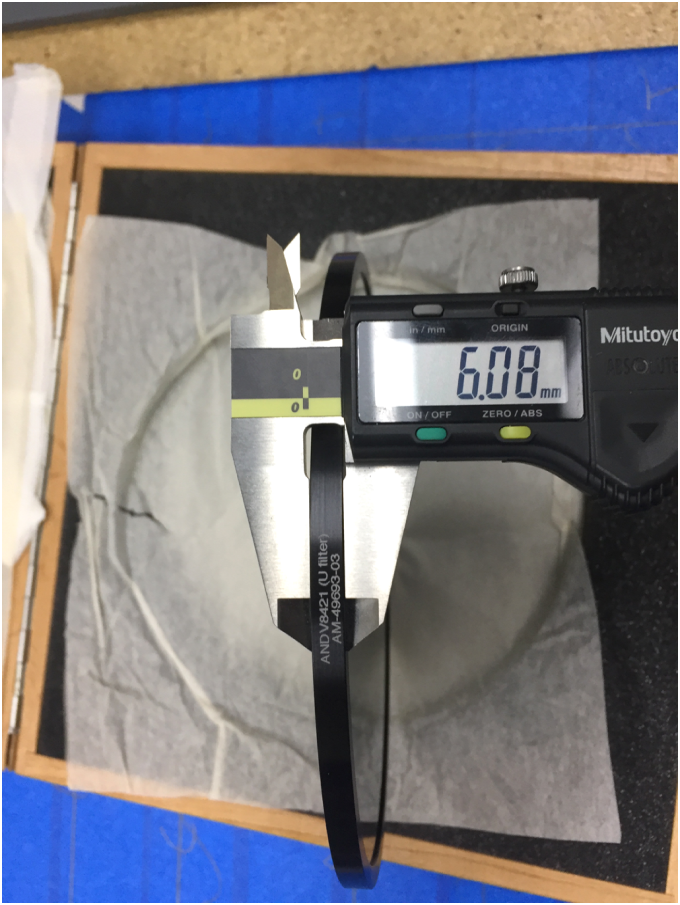
Example of metal banding with thinner substrate
Contact information
After approval of their program for queue observations with Gemini, the users should contact their assigned contact scientist regarding how to proceed with supplying their own filters. The contact scientist will put the users in contact with the appropriate Gemini Staff members.
Gratings
GMOS-N and GMOS-S use identical gratings and all gratings are available with each GMOS. However, some gratings are more heavily used than others and therefore spend more time in the instruments; see the grating statistics for recent semesters. Note in particular that the R600 grating has historically had very limited use and is now restricted to Classical programs only. Queue programs wishing to use this grating should consider whether their science requirements can be accommodated with the R400 or R831 grating instead.
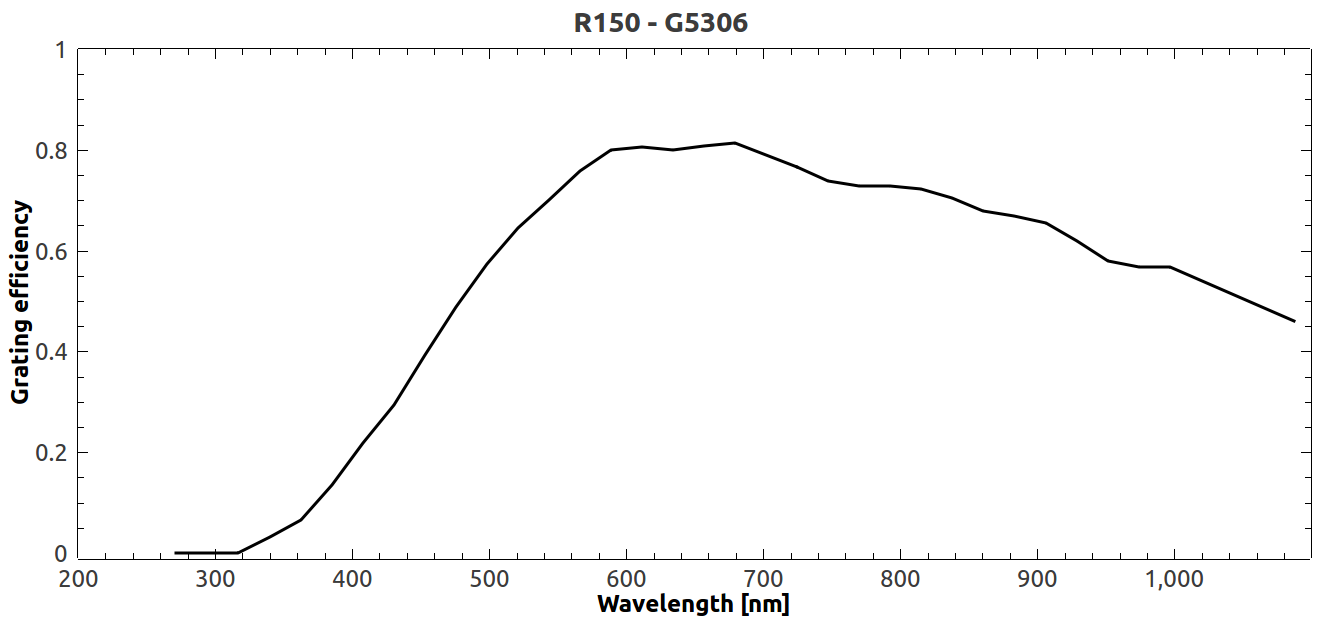
A new R150 grating has been available at GMOS-N since December 2016. See details here.
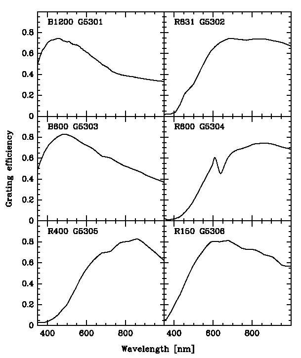
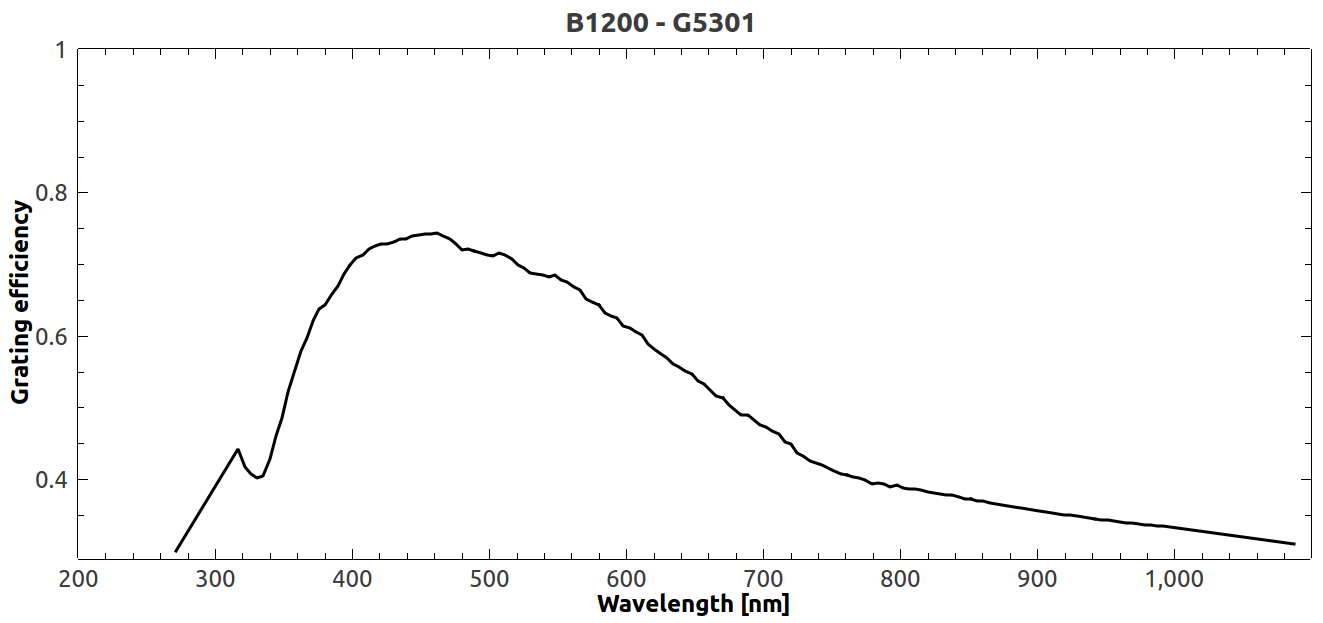
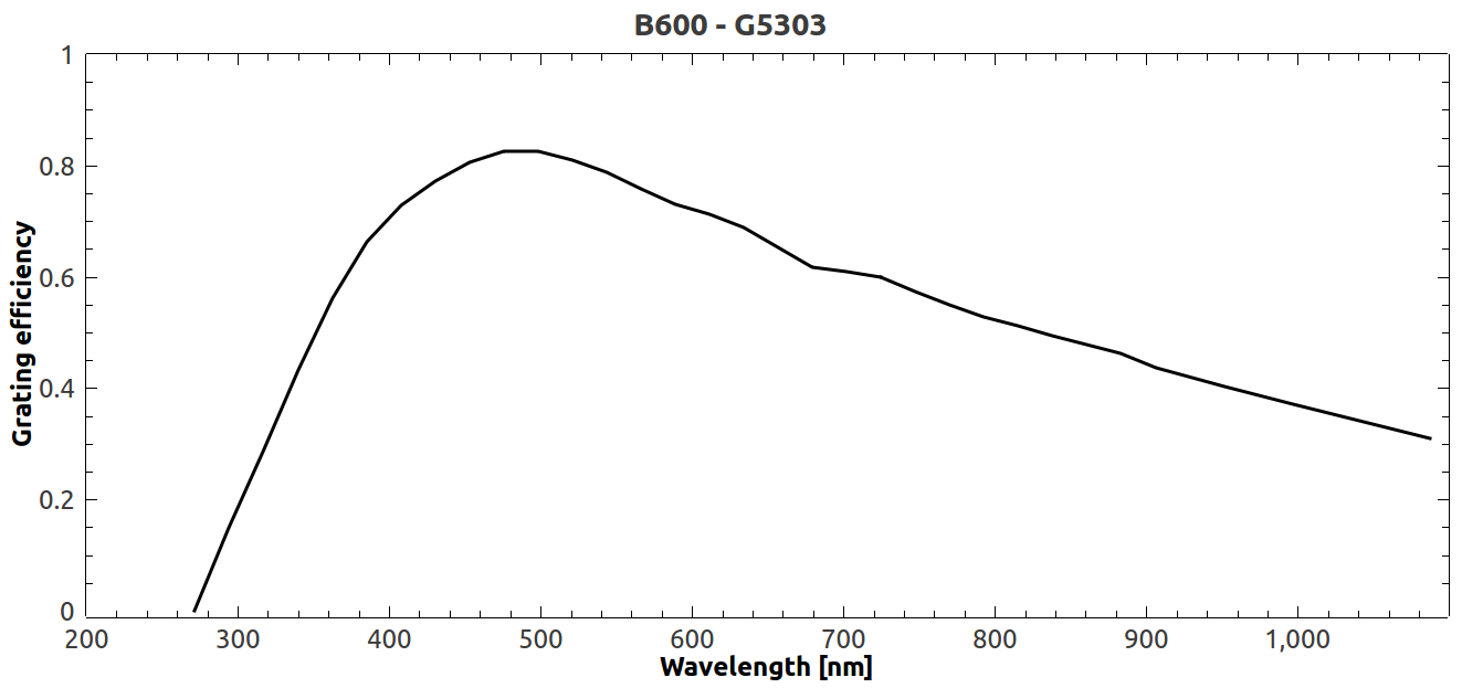
The table lists the properties of the GMOS gratings based on laboratory measurements. The resolving power R is given at the blaze wavelength, and refers to the resolution achieved with a slit width of 0.5 arcsec. The effective slit width of the IFU in the dispersion direction is 0.31arcsec, see the IFU grating/filter combination page for details.
Efficiency curves based on laboratory data are available. Note that the new GMOS-S Hamamatsu detectors have significant quantum efficiency at 1 µm, falling below 5 percent for wavelengths longer than ~ 1.07 µm (see GMOS-S Hamamatsu array page for more details). The quantum efficiency of the old GMOS-S EEV detectors was below 5 percent for wavelengths longer than 1000 nm. The grating efficiencies assumed by the GMOS-N ITC are extrapolations for wavelengths longer than 1 µm and will be updated once all the gratings have been characterized with the new GMOS-N Hamamatsu detectors. There is no laboratory data available for these gratings longward of 1 µm.
None of the gratings are currently officially offered in 2nd order; however tests have shown that the second order mode for the R600 and R831 gratings may be of interest for some applications. Contact your GMOS instrument scientist for more information.
| GMOS Gratings | |||||||
| Grating name | Grating number* | Ruling density [lines/mm] |
Blaze wavelength [nm] |
Resolutiona [R] |
Simultaneous coverage*** [nm] |
Dispersion [nm/pixel] |
Grating efficiency |
| GMOS-N |
GMOS-N / S e2v |
GMOS-N / S e2v | |||||
| GMOS-S | GMOS-N / S Hamamatsu |
GMOS-N / S Hamamatsu |
|||||
| B1200 | G5301 | 1200 | 463 | 3744 | 143 | 0.023 | data/plot |
| G5321 | 164 / 159 | 0.026 | |||||
| R831 | G5302 | 831 | 757 | 4396 | 207 | 0.034 | data/plot |
| G5322 | 235 / 230 | 0.038 | |||||
| B600c | (strongly degraded performance) G5307 |
600 | 461 | 1688 | 276 | 0.045 | data/plot |
| G5323 | 317 / 307 | 0.050 | |||||
| R600** | G5304 | 600 | 926 | 3744 | 286 | 0.047 | data/plot |
| G5324 | 328 / 318 | 0.052 | |||||
| R400 | G5305 | 400 | 764 | 1918 | 416 | 0.067 | data/plot |
| G5325 | 472 / 462 | 0.074 | |||||
|
R150**** |
(G5306 replaced 12/2016) G5308 |
150 | 717 | 631 | 1071 | 0.174 | |
| G5326 | 1219 / 1190 | 0.193 | |||||
|
B480 b |
G5309 | 480 | 422 | 1522 | N/A | N/A | |
| G5327 | 396 / 391 | 0.062 | |||||
*The grating name is the concatenation of grating and grating number e.g.R831_G5302 for the Gemini North R831 grating.
**The R600 grating is under-utilized and queue programs may have difficulty with completion due to competition for the three grating slots from the other five gratings. Hence the R600 grating is not available for regular queue programs. Classical programs may still request the R600 grating.
*** The coverage in the Hamamatsu array is broader for GMOS-N due to wider chip gaps.
**** For short central wavelength settings the zero-order from the R150 grating is shifted onto the detector. The zero order does not affect the spectrum for long-slit spectroscopy but leads to a contamination in data taken with the IFU 2-slit mode or with certain packed mask designs in multi-object spectroscopy mode. Details on the zero-order contamination in IFU-2 data can be found here. The zero-order contamination for packed mask designs is described here.
a The resolving power R is given at the blaze wavelength, and refers to the resolution achieved with a slit width of 0.5 arcsec. The effective slit width of the IFU in the dispersion direction is 0.31 arcsec.
b Although the blaze wavelength is to the blue, when coupled with the CCD response the effective sensitivity is balanced across the 400nm-900nm interval. The gratings are already included in the GMOS integration time calculators.
c The GMOS-N B600 grating has degraded significantly. Users are advised to consider alternative grating options, particularly the B480 grating which is similar to B600. The GMOS-S B600 grating is not affected.
Gratings 2nd order
Any of the GMOS gratings can be used in 2nd order; however only a few configurations are potentially interesting and none have been fully characterized. Prompted by a recent inquiry from the user community, we have recently made some daytime testing of the R831 grating in 2nd order. This mode offers higher resolution than delivered by the B1200 grating although the wavelength range is limited by the necessity to use broad-band color filters to block 1st order. Neither GMOS is currently equipped with red-blocking (short-pass) filters.
The configuration tested was R831 in 2nd order, central wavelength = 440 nm, using the g'-filter for order blocking. A Nod&Shuffle 1.0arcsec longslit data was used, which allowed for a characterization of scattered light beyond the edge of the slit. The detector was binned 2x2. The test data are available for download from the Gemini Observatory Archive. These test data were taken with GMOS-N:
| Filename | Grating Configuration | Data Type |
| N20110923S0129 | B1200 1st order | GCALflat |
| N20110923S0130 | B1200 1st order | CuAr |
| N20110923S0467 | R831 2nd order | GCALflat |
| N20110923S0468 | R831 2nd order | CuAr |
These daytime tests were encouraging, and users whose science would benefit from higher resolution and do not need full wavelength coverage may wish to consider this combination. The R831 grating efficiency in 2nd order is comparable to that of the B1200 grating in 1st order. The g-filter unfortunately introduces a drop in throughput of about 15% because its peak transmission is 85%. The resolution compared to the B1200 grating increases by about 40% as expected, and the amount of scattered light contribution per pixel is comparable.
Please note: we have yet to confirm the behavior of the Gemini GMOS IRAF data reduction scripts with 2nd order spectral data.
![[B1200 1st order GCALflat]](/sciops/instruments/gmos/B1200_440_g_1st_flat.jpg "B1200 1st order GCALflat")
![[R831 2nd order GCALflat]](/sciops/instruments/gmos/R831_440_g_2nd_flat.jpg "R831 2nd order GCALflat")
![[B1200 1st order CuAr]](/sciops/instruments/gmos/B1200_440_g_1st_CuAr_full.jpg "B1200 1st order CuAr")
![[R831 2nd order CuAr]](/sciops/instruments/gmos/R831_440_g_2nd_CuAr_full.jpg "R831 2nd order CuAr")
![[B1200 1st order CuAr (zoomed in)]](/sciops/instruments/gmos/B1200_440_g_1st_CuAr_zoom.jpg "B1200 1st order CuAr (zoomed in)")
![[R831 2nd order CuAr (zoomed in)]](/sciops/instruments/gmos/R831_440_g_2nd_CuAr_zoom.jpg "R831 2nd order CuAr (zoomed in)")
Long-slit Dimensions
Both GMOSs have a number of 'permanent' masks containing slits suitable for long-slit spectroscopy, for both standard and Nod-and-Shuffle observations. The slits have small bridges, approximately 3 arcsec long, to keep the mask flat in the focal plane (see the image in the table below).
The long slits for standard observations have length of 330 arcsec and various widths ranging from 0.25 arcsec to 5.0 arcsec. The Nod-and-Shuffle slits have lengths of 108 arcsec centered in the field of view, and are only available in slit widths of 0.5, 0.75, 1.0, 1.5 and 2.0 arcsec.
If users require slit widths other than the permanent ones listed below, or long-slit masks with holes for alignment objects, such requests will be handled as multi-object spectroscopy and the user should request to use GMOS in MOS mode. The user will have to prepare the masks using the usual mask-making procedure. A total of 18 masks (plus the IFU) can be loaded into GMOS at any given time.
| Slit width | Slit length(s) | Plot |
| 0.25 arcsec | 330 arcsec | |
| 0.5 arcsec | 330 and 108 arcsec | GIF image |
| 0.75 arcsec | 330 and 108 arcsec | |
| 1.0 arcsec | 330 and 108 arcsec | |
| 1.5 arcsec | 330 and 108 arcsec | |
| 2.0 arcsec | 330 and 108 arcsec | |
| 5.0 arcsec | 330 arcsec |